MIT-6.175 简介/目录
什么是 6.175?
6.175 通过实现不同版本的带缓存、分支预测和虚拟内存的流水线机器,教授计算机架构的基本原理。强调编写和评估可以模拟和合成到真实硬件或在 FPGA 上运行的架构描述。使用和设计测试台。本课程适合想要将计算机科学技术应用于复杂硬件设计的学生。
课题包括组合电路(包括加法器和乘法器)、多周期和流水线功能单元、RISC 指令集架构 (ISA)、非流水线和多周期处理器架构、2 至 10 阶段顺序流水线架构、带缓存和层次内存系统的处理器、TLB 和页面错误、I/O 中断。
讲师
- Arvind
- Quan Nguyen (助教)
讲座
周一周三周五 下午 3:00, 34-302。
实验课程目录
- MIT-6.175 简介/目录
- 实验 0: 入门
- 实验 1: 多路选择器和加法器
- 实验 2: 乘法器
- 实验 3: 快速傅里叶变换管道
- 实验 4: N 元 FIFOs
- 实验 5: RISC-V 引介 - 多周期与两阶段流水线
- 实验 6: 具有六阶段流水线和分支预测的 RISC-V 处理器
- 实验 7: 带有 DRAM 和缓存的 RISC-V 处理器
- 实验 8: 具有异常处理的 RISC-V 处理器
项目
日程安排
| 周数 | 日期 | 描述 | 下载链接 |
|---|---|---|---|
| 1 | 周三, 9月7日 | 讲座 1: 介绍 | [pptx] [pdf] |
| 周五, 9月9日 | 讲座 2: 组合电路 实验 0 发布, 实验 1 发布 | [pptx] [pdf] | |
| 2 | 周一, 9月12日 | 讲座 3: 组合电路 2 | [pptx] [pdf] |
| 周三, 9月14 | 讲座 4: 时序电路 | [pptx] [pdf] | |
| 周五, 9月16 | 讲座 5: 时序电路 2 实验 1 截止, 实验 2 发布 | [pptx] [pdf] | |
| 3 | 周一, 9月19日 | 讲座 6: 组合电路的流水线化 | [pptx] [pdf] |
| 周三, 9月21日 | 讲座 7: 基本良好的 BSV 程序 短暂历史寄存器 | [pptx] [pdf] | |
| 周五, 9月23日 | 无课: 学生假日 (秋季招聘会) 实验 3 发布 | ||
| 4 | 周一, 9月26日 | 讲座 8: 多规则系统与规则的并发执行 实验 2 截止 | [pptx] [pdf] |
| 周三, 9月28日 | 讲座 9: 保护条件 | [pptx] [pdf] | |
| 周五, 9月30日 | 辅导课 1: Bluespec | [pptx] [pdf] | |
| 5 | 周一, 10月3 | 讲座 10: 非流水线处理器 实验 4 发布 | [pptx] [pdf] |
| 周三, 10月5日 | 讲座 11: 非流水线和流水线处理器 实验 3 截止 | [pptx] [pdf] | |
| 周五, 10月7日 | 辅导课 2: 高级 Bluespec | [pptx] [pdf] | |
| 6 | 周一, 10月10日 | 无课: 原住民日 / 哥伦布日 | |
| 周二, 10月11日 | 实验 5 发布 | ||
| 周三, 10月12日 | 讲座 12: 控制冒险 实验 4 截止 | [pptx] [pdf] | |
| 周五, 10月14 | 辅导课 3: RISC-V 处理器 RISC-V 和调试 | [pptx] [pdf] | |
| 7 | 周一, 10月17日 | 讲座 13: 数据冒险 | [pptx] [pdf] |
| 周三, 10月19日 | 讲座 14: 多阶段流水线 实验 6 发布 | [pptx] [pdf] | |
| 周五, 10月21日 | 辅导课 4: 调试时代和记分板 实验 5 截止 | [pptx] [pdf] | |
| 8 | 周一, 10月24日 | 讲座 15: 分支预测 实验 5 截止 | [pptx] [pdf] |
| 周三, 10月26日 | 讲座 16: 分支预测 2 | [pptx] [pdf] | |
| 周五, 10月28日 | 辅导课 5: 时代和分支预测器 时代、调试和缓存 | [pptx] [pdf] | |
| 9 | 周一, 10月31日 | 讲座 17: 缓存 | [pptx] [pdf] |
| 周三, 11月2日 | 讲座 18: 缓存 2 实验 7 发布 | [pptx] [pdf] | |
| 周五, 11月4日 | 辅导课 6: 缓存和异常 实验 6 截止 | [pptx] [pdf] | |
| 10 | 周一, 11月7日 | 讲座 19: 异常 实验 6 截止 | [pptx] [pdf] |
| 周三, 11月9日 | 讲座 20: 虚拟内存 | [pptx] [pdf] | |
| 周五, 11月11日 | 无课: 退伍军人节 | ||
| 11 | 周一, 11月14日 | 讲座 21: 虚拟内存和异常 实验 8 发布 | [pptx] [pdf] |
| 周三, 11月16日 | 讲座 22: 缓存一致性 实验 7 截止 | [pptx] [pdf] | |
| 周四, 11月17日 | 实验 8 发布 | ||
| 周五, 11月18日 | 辅导课 7: 项目概述 实验 7 截止, 项目第一部分 发布 | [pptx] [pdf] | |
| 12 | 周一, 11月21日 | 讲座 23: 顺序一致性 | [pptx] [pdf] |
| 周三, 11月23日 | 辅导课 8: 项目第二部分: 一致性 取消: (提前) 感恩节 实验 8 截止 | ||
| 周五, 11月25日 | 无课: 感恩节 实验 8 截止 | ||
| 13 | 周一, 11月28日 | 无课: 从事项目 项目第二部分发布 | |
| 周三, 11月30日 | 无课: 从事项目 | ||
| 周四, 12月1日 | 项目第二部分 发布 | ||
| 周五, 12月2日 | 无课: 从事项目 辅导课 8: 项目第二部分: 一致性 | [pptx] [pdf] | |
| 14 | 周一, 12月5日 | 无课: 从事项目 | |
| 周三, 12月7日 | 无课: 从事项目 | ||
| 周五, 12月9日 | 无课: 从事项目 | ||
| 15 | 周一, 12月12日 | 无课: 从事项目 | |
| 周三, 12月14日 | 课程最后一天 项目展示 |
© 2016 麻省理工学院 版权所有。
实验 0: 入门
在本课程中,你将使用共享机器来完成实验。这些机器包括从 vlsifarm-03.mit.edu 到 vlsifarm-08.mit.edu。你可以通过使用你的Athena用户名和密码通过ssh登录这些机器。
本文档将指导你完成实验所需的一些操作,如获取每个实验的初始代码。首先使用ssh客户端登录上述任一服务器。
设置工具链
执行以下命令来设置你的环境并访问工具链:
add 6.175
source /mit/6.175/setup.sh
第一个命令使你能够访问课程锁定目录 /mit/6.175,并且每台电脑只需运行一次。第二个命令配置你当前的环境以包括实验所需的工具,每次登录工作时都需要运行。
使用Git获取和提交实验代码
参考设计提供在Git仓库中。你可以使用以下命令将它们克隆到你的工作目录中(用实验编号替换 labN,例如 lab1 和 lab2):
git clone $GITROOT/labN.git
注意:如果 "git clone" 失败,可能是因为我们没有你的Athena用户名。请给我发送电子邮件(至 qmn mit),我将为你创建一个远程仓库。
此命令在你当前目录中创建一个 labN 目录。$GITROOT 环境变量是唯一的,因此这个仓库将是你个人的仓库。在该目录中,可以使用实验讲义中指定的指令运行测试台。
讨论问题应该在提供的代码中的 discussion.txt 文件中回答。
如果你想添加任何新文件,除了助教提供的文件外,你需要使用以下命令添加新文件(在这个例子中,是 git 中的 newFile):
git add newFile
你可以在达到一个里程碑时本地提交你的代码:
git commit -am "Hit milestone"
通过添加任何必要的文件然后使用以下命令提交你的代码:
git commit -am "Finished lab"
git push
如有必要,你可以在截止日期前多次提交。
编写实验的Bluespec SystemVerilog(BSV)代码
在 vlsifarm-0x 上
如果你还不熟悉Linux命令行环境,6.175将是一个很好的学习机会。测试你的BSV代码,你需要在Linux环境下运行bsc,即BSV编译器。在同一台机器上编写BSV代码是有意义的。
虽然你可以使用许多文本编辑器,但只有Vim和Emacs为Bluespec提供了BSV语法高亮。Vim语法高亮文件可以通过运行以下命令安装:
/mit/6.175/vim_copy_BSV_syntax.sh
Emacs语法高亮文件可以在课程资源页面找到。你的助教曾经使用Emacs,但后来转用了Vim。他无法声称知道如何安装高亮模式文件,甚至是否有效。如果你是Emacs用户并愿意就此事贡献文档,请发邮件给课程工作人员。
在 Athena 集群上
你在 vlsifarm 机器上的家目录与任何 Athena 机器上的家目录相同。因此,你可以在Athena机器上使用gedit或其他图形文本编辑器编写代码,然后登录到vlsifarm机器上运行它。
在你自己的机器上
你也可以使用文件传输程序在
你的Athena家目录和你自己的机器之间移动文件。MIT在网上提供了关于安全传输文件的帮助,网址为 http://ist.mit.edu/software/filetransfer。
在其他机器上编译BSV
BSV也可以在非vlsifarm机器上编译。这在实验截止日期临近时vlsifarm机器繁忙时可能很有用。
在 Athena 集群上
用于vlsifarm机器的指令也适用于基于Linux的Athena机器。只需打开一个终端,像在vlsifarm机器上一样运行命令即可。
在你自己的基于Linux的机器上
要在你自己的基于Linux的机器上运行6.175实验,你需要在计算机上安装以下软件:
- OpenAFS以访问课程锁定目录
- Git以访问和提交实验
- GMP (libgmp.so.3)以运行BSV编译器
- Python以运行构建脚本
旁注:类似的设置也可能适用于Mac OS X / macOS。如果你让这样的设置工作,请向助教提供详细信息。
OpenAFS
在你的本地机器上安装OpenAFS将使你能够访问包含所有课程锁定目录的目录 /afs/athena.mit.edu。你将需要在根目录中创建一个名为/mit的文件夹,并在其中使用符号链接指向必要的课程锁定目录。
CSAIL TIG有一些关于如何为Ubuntu安装OpenAFS的信息,网址为 http://tig.csail.mit.edu/wiki/TIG/OpenAFSOnUbuntuLinux。这些指令用于访问 /afs/csail.mit.edu,但你需要访问 /afs/athena.mit.edu 来进行实验,所以无论何时看到csail都用athena替换。当你在你的机器上安装OpenAFS时,它会给你一个包含许多域的 /afs 文件夹。此网站还包含了使用你的用户名和密码登录以获取需要身份验证的文件的指令。你需要每天工作或每次重置计算机时都执行此操作,以便访问6.175课程锁定目录。
接下来你需要在根目录创建一个名为mit的文件夹,并在其中填充指向课程仓库的符号链接。在Ubuntu和类似的分发版上,命令如下:
cd /
sudo mkdir mit
cd mit
sudo ln -s /afs/athena.mit.edu/course/6/6.175 6.175
现在你可以在 /mit/6.175 文件夹中访问课程锁定目录了。
Git
在Ubuntu和类似的分发版上,你可以用以下命令安装Git:
sudo apt-get install git
GMP (libgmp.so.3)
BSV编译器使用libgmp来处理无界整数。在Ubuntu和类似的分发版上安装它,使用命令:
sudo apt-get install libgmp3-dev
如果你的机器上安装了libgmp,但你没有libgmp.so.3,你可以创建一个名为libgmp.so.3的符号链接,指向不同版本的libgmp。
Python
在Ubuntu和类似的分发版上,你可以使用以下命令安装Python:
sudo apt-get install python
在你基于Linux的机器上设置工具链
原始的 setup.sh 脚本在你的机器上不会工作,所以你将需要使用
source /mit/6.175/local_setup.sh
来设置工具链。完成这些后,你应该能够像在你自己的机器上
一样正常使用这些工具。
© 2016 麻省理工学院。版权所有。
实验 1: 多路选择器和加法器
实验 1 截止日期: 2016年9月16日,星期五,晚上11:59:59 EDT。
实验 1 的交付物包括:
- 在
Multiplexer.bsv和Adders.bsv中对练习 1-5 的回答,- 在
discussion.txt中对讨论问题的回答。
引言
在本实验中,你将从基本门原语构建多路选择器和加法器。首先,你将使用与门、或门和非门构建一个 1 位多路选择器。接下来,你将使用 for 循环编写一个多态性多路选择器。然后,你将转向加法器的工作,使用全加器构建一个 4 位加法器。最后,你将修改一个 8 位行波进位加法器,将其改为选择进位加法器。
本实验用作简单组合电路和 Bluespec SystemVerilog (BSV) 的引入。尽管 BSV 包含用于创建电路的高级功能,本实验将侧重于使用低级门来创建用于高级电路的块,例如加法器。这强调了 BSV 编译器生成的硬件。
多路选择器
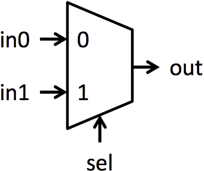
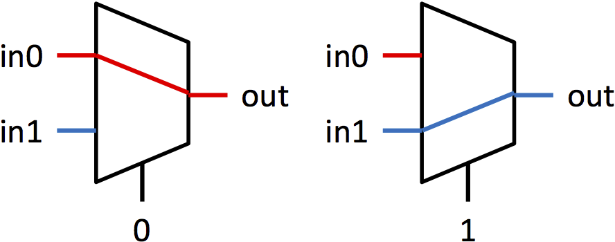
多路选择器(简称 muxes)是在多个信号之间选择的块。多路选择器有多个数据输入 inN,一个选择输入 sel,和一个单一输出 out。sel 的值决定哪个输入显示在输出上。本实验中的多路选择器都是 2 路多路选择器。这意味着将有两个输入可以选择(in0 和 in1),并且 sel 是一个单一位。如果 sel 为 0,则 out = in0;如果 sel 为 1,则 out = in1。图 1a 显示了用于多路选择器的符号,图 1b 以图形方式显示了多路选择器的功能。
 |  |
|---|---|
| (a) 多路选择器符号 | (b) 多路选择器功能 |
图 1:1 位多路选择器的符号和功能
加法器
加法器是数字系统的基本构建块。有许多不同的加法器架构都可以计算相同的结果,但它们以不同的方式达到结果。不同的加法器架构在面积、速度和功耗方面也有所不同,并且没有一种架构在所有领域都超越其他加法器。因此,硬件设计师根据系统面积、速度和功耗约束选择加法器。
我们将探索的加法器架构是行波进位加法器和选择进位加法器。行波进位加法器是最简单的加法器架构。它由通过进位链连接的全加器块链组成。图 2b 中可以看到一个 4 位行波进位加法器。它非常小,但也非常慢,因为每个全加器必须等待前一个全加器完成后才能计算其位。
选择进位加法器为行波进位加法器添加了预测或推测以加快执行速度。它以与行波进位加法器相同的方式计算底部位,但计算顶部位的方式不同。它不等待来自下面位的进位信号计算,而是计算顶部位的两个可能结果:一个
假设下面的位没有进位,另一个假设有进位。一旦计算出进位位,多路选择器就会选择与进位位相对应的顶部位。图 3 中可以看到一个 8 位选择进位加法器。
 |  |
|---|---|
| (a) 全加器 | (b) 由全加器构建的 4 位行波进位加法器 |
 |  |
|---|---|
| (c) 4 位加法器符号 | (d) 8 位行波进位加法器 |
图 2:由全加器块构建的 4 位加法器和 8 位加法器
 |
|---|
图 3:8 位选择进位加法器
测试台
已经编写了用于测试你的代码的测试台,测试台的链接包含在本实验的仓库中。文件 TestBench.bsv 包含多个可以使用提供的 Makefile 单独编译的测试台。Makefile 有每个模拟器可执行文件的目标,每个目标和可执行文件的使用在本手册中进行了解释。每个可执行文件在程序工作时打印出 PASSED,在程序遇到错误时打印出 FAILED。
以 Simple 结尾的测试台结构简化了,并且它们输出了来自单元测试期间单元的所有数据,以便你可以看到单元的工作情况。如果你有兴趣测试这些单元的自己的案例,你可以修改简单的测试台以输入你请求的值。普通测试台会为输入值生成随机数。
在 BSV 中构建多路选择器
构建我们的选择进位加法器的第一步是从门构建一个基本的多路选择器。让我们首先检查 Multiplexer.bsv。
function Bit#(1) multiplexer1(Bit#(1) sel, Bit#(1) a, Bit#(1) b);
    return (sel == 0)? a: b;
endfunction
第一行开始定义一个名为 multiplexer1 的新函数。这个多路选择器函数接收几个参数,这些参数将用于定义多路选择器的行为。这个多路选择器操作单比特值,具体类型 Bit#(1)。稍后我们将学习如何实现多态函数,这些函数可以处理任何宽度的参数。
这个函数在其定义中使用了类似 C 的构造。如多路选择器这样简单的代码可以在高层次上定义,而不会带来实现上的惩罚。然而,由于硬件编译是一个复杂的多维问题,工具在它们可以执行的优化类型上是有限的。
return 语句构成了整个函数,它接收两个输入并使用 sel 选择其中之一。endfunction 关键字完成了我们多路选择器函数的定义。你应该能够编译该模块。
练习 1(4 分): 使用与门、或门和非门重新实现函数
multiplexer1 在 Multiplexer.bsv 中。需要多少个门?(所需的函数分别称为 and1、or1 和 not1,在 Multiplexers.bsv 中提供。)
静态展开
现实世界系统中的许多多路选择器都大于 1 位宽。我们需要大于单比特的多路选择器,但手动实例化 32 个单比特多路选择器以形成一个 32 位多路选择器将是乏味的。幸运的是,BSV 提供了强大的静态展开构造,我们可以使用它来简化编写代码的过程。静态展开是指 BSV 编译器在编译时评估表达式的过程,使用结果来生成硬件。静态展开可以用几行代码表达极其灵活的设计。
在 BSV 中,我们可以使用方括号 ([]) 索引更宽 Bit 类型中的单个位,例如 bitVector[1] 选择 bitVector 中的第二个最低有效位(bitVector[0] 选择最低有效位,因为 BSV 的索引从 0 开始)。我们可以使用 for 循环来复制许多具有相同形式的代码行。例如,要聚合 and1 函数形成一个 5 位 and 函数,我们可以写:
function Bit#(5) and5(Bit#(5) a, Bit#(5) b); Bit#(5) aggregate;
    for(Integer i = 0; i < 5; i = i + 1) begin
        aggregate[i] = and1(a[i], b[i]);
    end
    return aggregate;
endfunction
BSV 编译器在其静态展开阶段会用其完全展开的版本替换这个 for 循环。
aggregate[0] = and1(a[0], b[0]);
aggregate[1] = and1(a[1], b[1]);
aggregate[2] = and1(a[2], b[2]);
aggregate[3] = and1(a[3], b[3]);
aggregate[4] = and1(a[4], b[4]);
练习 2(1 分): 使用 for 循环和
multiplexer1完成函数multiplexer5在Multiplexer.bsv中的实现。 通过运行多路选择器测试台检查代码的正确性:$ make mux $ ./simMux可以使用另一个测试台来查看单元的输出:
$ make muxsimple
$ ./simMuxSimple
多态性和高阶构造器
到目前为止,我们已经实现了两个版本的多路选择器函数,但可以想象需要一个 n 位多路选择器。如果我们不必完全重新实现多路选择器就能使用不同的宽度,那将是很好的。使用前一节中介绍的 for 循环,我们的多路选择器代码已经有些参数化,因为我们使用了常数大小和相同类型。我们可以通过使用 typedef 给多路选择器的大小起一个名字(N)来做得更好。我们的新多路选择器代码看起来像这样:
typedef 5 N;
function Bit#(N) multiplexerN(Bit#(1) sel, Bit#(N) a, Bit#(N) b);
    // ...
    // 从 multiplexer5 中的代码,用 N(或 valueOf(N))替换 5
    // ...
endfunction
typedef 使我们能够随意更改多路选择器的大小。valueOf 函数在我们的代码中引入了一个小细节:N 不是一个 Integer 而是一个 数值类型,必须在用于表达式之前转换为 Integer。尽管有所改进,我们的实现仍然
缺乏一些灵活性。所有多路选择器的实例必须具有相同的类型,我们仍然必须为每次想要新的多路选择器时产生新代码。然而在 BSV 中,我们可以进一步参数化模块以允许不同的实例具有实例特定的参数。这种模块是多态的,硬件的实现会根据编译时配置自动改变。多态性是 BSV 设计空间探索的本质。
真正的多态多路选择器可以从以下开始:
// typedef 32 N; // 不需要
function Bit#(n) multiplexer n(Bit#(1) sel, Bit#(n) a, Bit#(n) b);
变量 n 代表多路选择器的宽度,替换了具体值 N(=32)。在 BSV 中,类型变量(n)以小写字母开头,而具体类型(N)以大写字母开头。
练习 3(2 分): 完成函数
multiplexer_n的定义。通过将原始定义的multiplexer5只更改为:return multiplexer_n(sel, a, b);来验证此函数的正确性。这种重新定义允许测试台在不修改的情况下测试你的新实现。
在 BSV 中构建加法器
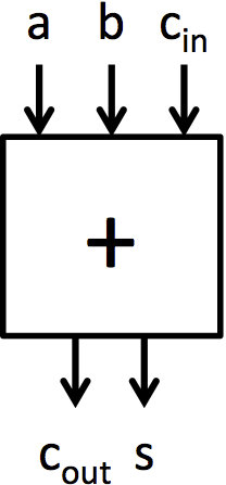
现在我们将转向构建加法器。加法的基本单元是全加器,如图 2a 所示。这个单元将两个输入位和一个进位输入位相加,它产生一个和位和一个进位输出位。Adders.bsv 包含两个函数定义,描述了全加器的行为。fa_add 计算全加器的加法输出,fa_carry 计算进位输出。这些函数包含与第 2 讲中呈现的全加器相同的逻辑。
可以通过将 4 个全加器连接在一起制作一个操作 4 位数的加法器,如图 2b 所示。这种加法器架构被称为行波进位加法器,因为进位链的结构。为了生成这种加法器而不写出每个显式的全加器,可以使用类似于 multiplexer5 的 for 循环。
练习 4(2 分): 使用 for 循环正确连接所有使用
fa_sum和fa_carry的代码来完成add4的代码。
通过连接 4 位加法器,可以构建更大的加法器,就像通过连接全加器构建 4 位加法器一样。Adders.bsv 包含两个使用 add4 和连接电路构建的加法器模块:mkRCAdder 和 mkCSAdder。注意,与此点到的其他加法器不同,这些加法器是作为模块而不是函数实现的。这是一个微妙但重要的区别。在 BSV 中,函数由编译器自动内联,而模块必须使用 '<-' 符号显式实例化。如果我们将 8 位加法器制作成一个函数,使用它的 BSV 代码的多个位置将实例化多个加法器。通过将其制作成一个模块,多个来源可以使用相同的 8 位加法器。
在模块 mkRCAdder 中包含了图 2d 所示的 8 位行波进位加法器的完整实现。可以通过运行以下命令进行测试:
make rca
./simRca
由于 mkRCAdder 是通过组合 add4 实例构建的,运行 ./simRCA 也将测试 add4。可以使用另一个测试台来查看单元的输出:
$ make rcasimple
$ ./simRca

Simple
还有一个 mkCSAdder 模块,旨在实现图 3 所示的选择进位加法器,但其实现未包含。
练习 5(5 分): 在模块
mkCSAdder中完成选择进位加法器的代码。使用图 3 作为所需硬件和连接的指南。可以通过运行以下命令测试此模块:$ make csa $ ./simCsa可以使用另一个测试台来查看单元的输出:
$ make csasimple
$ ./simCsaSimple
讨论问题
在初始实验代码提供的文本文件
discussion.txt中写下对这些问题的回答。
- 你的一位多路选择器使用了多少个门?5 位多路选择器呢?写下 N 位多路选择器中门的数量的公式。(2 分)
- 假设一个全加器需要 5 个门。8 位行波进位加法器需要多少个门?8 位选择进位加法器需要多少个门?(2 分)
- 假设一个全加器需要 A 时间单位来计算其输出,一旦所有输入都有效,一个多路选择器需要 M 时间单位来计算其输出。用 A 和 M 表示,8 位行波进位加法器需要多长时间?8 位选择进位加法器需要多长时间?(2 分)
- 可选:你花了多长时间来完成这个实验?
完成后,使用 git add 添加任何必要的文件,使用 git commit -am "Final submission" 提交更改,并用 git push 推送修改以进行评分。
© 2016 麻省理工学院。版权所有。
实验 2: 乘法器
实验 2 截止日期: 2016年9月26日星期一,晚上11:59:59 EDT。 你的实验 2 交付物包括:
- 在
Multipliers.bsv和TestBench.bsv中对练习 1-9 的回答,- 在
discussion.txt中对讨论问题 1-5 的回答。
引言
在本实验中,你将构建不同的乘法器实现,并使用提供的测试台模板的自定义实例进行测试。首先,你将使用重复加法实现乘法器。接下来,你将使用折叠架构实现一个布斯乘法器。最后,你将通过实现一个基-4 布斯乘法器来构建一个更快的乘法器。
这些模块的输出将通过测试台与 BSV 的 * 操作符进行比较以验证功能。
本实验的所有材料都在 git 仓库 $GITROOT/lab2.git 中。本实验中提出的所有讨论问题都应该在 discussion.txt 中回答。完成实验后,将你的更改提交到仓库并推送更改。
内置乘法
BSV 具有内置的乘法操作:*。它是有符号或无符号乘法,具体取决于操作数的类型。对于 Bit#(n) 和 UInt#(n),* 操作符执行无符号乘法。对于 Int#(n),它执行有符号乘法。就像 + 操作符一样,* 操作符假设输入和输出都是同一类型。如果你想从 n 位操作数得到一个 2n 位结果,你必须首先将操作数扩展为 2n 位值。
Multipliers.bsv 包含了对 Bit#(n) 输入进行有符号和无符号乘法的函数。两个函数都返回 Bit#(TAdd#(n,n)) 输出。这些函数的代码如下所示:
注意:
pack和unpack是内置函数,分别用于转换为和从Bit#(n)转换。
function Bit#(TAdd#(n,n)) multiply_unsigned( Bit#(n) a, Bit#(n) b );
    UInt#(n) a_uint = unpack(a);
    UInt#(n) b_uint = unpack(b);
    UInt#(TAdd#(n,n)) product_uint = zeroExtend(a_uint) * zeroExtend(b_uint);
    return pack( product_uint );
endfunction

function Bit#(TAdd#(n,n)) multiply_signed( Bit#(n) a, Bit#(n) b );
    Int#(n) a_int = unpack(a);
    Int#(n) b_int = unpack(b);
    Int#(TAdd#(n,n)) product_int = signExtend(a_int) * signExtend(b_int);
    return pack( product_int );
endfunction
这些函数将作为你在本实验中的乘法器的功能基准进行比较。
测试台
本实验有两个参数化的测试台模板,可以很容易地用特定参数实例化,以测试两个乘法函数之间的对比,或测试一个乘法器模块与一个乘法器函数的对比。这些参数包括函数和模块接口。mkTbMulFunction 用相同的随机输入比较两个函数的输出,而 mkTbMulModule 比较测试模块(被测试设备或 DUT)和参考函数的输出。
以下代码展示了如何为特定的函数和/或模块实现测试台。
(* synthesize *)
module mkTbDumb();
    function Bit#(16) test_function( Bit#(8) a, Bit#(8) b ) = multiply_unsigned( a, b );
    Empty tb <- mkTbMulFunction

(test_function, multiply_unsigned, True);
    return tb;
endmodule

(* synthesize *)
module mkTbFoldedMultiplier();
    Multiplier#(8) dut <- mkFoldedMultiplier();
    Empty tb <- mkTbMulModule(dut, multiply_signed, True);
    return tb;
endmodule
下面两行使用 TestBenchTemplates.bsv 中的测试台模板实例化特定的测试台。
Empty tb <- mkTbMulFunction(test_function, multiply_unsigned, True);
Empty tb <- mkTbMulModule(dut, multiply_signed, True);
每个的第一个参数(test_function 和 dut)是要测试的函数或模块。第二个参数(multiply_unsigned 和 multiply_signed)是正确实现的参考函数。在这种情况下,参考函数是使用 BSV 的 * 操作符创建的。最后一个参数是一个布尔值,指示你是否希望输出详细信息。如果你只想让测试台打印 PASSED 或 FAILED,将最后一个参数设置为 False。
这些测试台(mkTbDumb 和 mkTbFoldedMultiplier)可以使用提供的 Makefile 轻松构建。要编译这些示例,你会为第一个写 make Dumb.tb,为第二个写 make FoldedMultiplier.tb。makefile 将产生可执行文件 simDumb 和 simFoldedMultiplier。要编译你自己的测试台 mkTb<name>,运行
make <name>.tb
./sim<name>
编译过程不会产生 .tb 文件,扩展名只是用来指示应使用哪个构建目标。
练习 1(2 分): 在
TestBench.bsv中编写一个测试台mkTbSignedVsUnsigned,测试multiply_signed是否产生与multiply_unsigned相同的输出。按上述描述编译此测试台并运行。 (即运行$ make SignedVsUnsigned.tb然后
$ ./simSignedVsUnsigned)
讨论问题 1(1 分): 在使用二的补码编码时,从硬件角度来看,无符号加法与有符号加法是相同的。根据测试台的证据,无符号乘法与有符号乘法是否相同?
讨论问题 2(2 分): 在
mkTBDumb中排除以下行function Bit#(16) test_function( Bit#(8) a, Bit#(8) b ) = multiply_unsigned( a, b );并修改其余的模块,以便拥有
(* synthesize *)
module mkTbDumb();
Empty tb <- mkTbMulFunction(multiply_unsigned, multiply_unsigned, True);
return tb;
endmodule
将导致编译错误。原始代码是如何修复编译错误的?你也可以通过定义两个函数来修复错误,如下所示。
(* synthesize *)
module mkTbDumb();
function Bit#(16) test_function( Bit#(8) a, Bit#(8) b ) = multiply_unsigned( a, b );
function Bit#(16) ref_function( Bit#(8) a, Bit#(8) b ) = multiply_unsigned( a, b );
Empty tb <- mkTbMulFunction(test_function, ref_function, True);
return tb;
endmodule
为什么不需要两个函数定义?(即为什么
mkTbMulFunction的第二个操作数可以有变量类型?)提示: 查看TestBenchTemplates.bsv中mkTbMulFunction的操作数类型。
通过重复加法实现乘法
作为组合函数
在 Multipliers.bsv 中,有一个用于计算乘法的函数框架代码,该函数通过重复加法来计算。由于这是一个函数,它必须代表一个组合电路。
练习 2(3 分): 填写
multiply_by_adding的代码,使其能够使用重复加法在一个时钟周期内计算 a 和 b 的乘积。(你将在练习 3 中验证你的乘法器的正确性。)如果你需要一个加法器从两个 n 位操作数产生一个 (n+1) 位输出,请按照multiply_unsigned和multiply_signed的模型,先将操作数扩展为 (n+1) 位再相加。
练习 3(1 分): 在
TestBench.bsv中填写测试台mkTbEx3来测试multiply_by_adding的功能。使用以下命令编译它:$ make Ex3.tb并使用以下命令运行它:
$ ./simEx3
讨论问题 3(1 分): 你实现的
multiply_by_adding是有符号乘法器还是无符号乘法器?(注意:如果它既不符合multiply_signed也不符合multiply_unsigned,那么它是错误的。)
作为顺序模块
使用重复加法乘以两个 32 位数需要三十一个 32 位加法器。这些加法器可能会根据你的目标和其余设计的限制占用大量面积。在讲座中,展示了重复加法乘法器的折叠版本,以减少乘法器所需的面积。折叠版本的乘法器使用顺序电路,通过每个时钟周期完成一个所需计算并将临时结果存储在寄存器中,来共享单个 32 位加法器。
在本实验中,我们将创建一个 n 位折叠乘法器。寄存器 i 将跟踪模块在计算结果中的进度。如果 0 <= i < n,则正在进行计算,规则 mul_step 应该在做工作并递增 i。有两种方法可以做到这一点。第一种方法是制作一个包含 if 语句的规则,如下所示:
rule mul_step;
    if (i < fromInteger(valueOf(n))) begin
        // 做一些事情
    end
endrule
这个规则每个周期都运行,但只有当 i < n 时才做事情。第二种方法是制作一个带有 保护 的规则,如下所示:
rule mul_step(i < fromInteger(valueOf(n)));
    // 做一些事情
endrule
这个规则不会每个周期都运行。相反,它只在其保护,i < fromInteger(valueOf(i)),为真时运行。虽然这在功能上没有区别,但在 BSV 语言的语义和编译器中有所不同。这种差异将在后续讲座中讨论,但在此之前,你应该在本实验的设计中使用保护。如果不这样做,你可能会遇到测试台因为运行超时而失败。
注意: BSV 编译器防止多个规则在同一周期内触发,如果它们可能写入同一个寄存器(有点类似...)。BSV 编译器将规则
mul_step视为每次触发时都写入i。测试台中有一个规
则用于向乘法器模块提供输入,因为它调用了 start 方法,所以它也每次触发时都写入 i。BSV 编译器看到这些冲突的规则,并发出编译器警告,它将把一个规则视为比另一个更紧急,永远不会同时触发它们。它通常选择 mul_step,由于该规则每个周期都触发,它阻止了测试台规则向模块提供输入。
当 i 达到 n 时,结果已准备好读取,因此 result_ready 应返回 true。当调用动作值方法 result 时,i 的状态应增加 1 至 n+1。i == n+1 表明模块准备重新开始,因此 start_ready 应返回 true。当调用动作方法 start 时,模块中所有寄存器的状态(包括 i)应设置为正确的值,以便重新开始计算。
练习 4(4 分): 填写模块
mkFoldedMultiplier的代码,以实现一个折叠的重复加法乘法器。你能在不使用变量位移位移器的情况下实现它吗?在不使用动态位选择的情况下实现它吗?(换句话说,你能避免通过存储在寄存器中的值进行位移或位选择吗?)
练习 5(1 分): 填写测试台
mkTbEx5以测试mkFoldedMultiplier的功能。如果你正确实现了mkFoldedMultiplier,它们应产生相同的输出。运行它们,使用:$ make Ex5.tb $ ./simEx5
布斯乘法算法
重复加法算法适用于乘以无符号输入,但它无法乘以使用二进制补码编码的(负)数字。为了乘以有符号数字,你需要一个不同的乘法算法。
布斯乘法算法是一种适用于有符号二进制补码数的算法。该算法使用一种特殊的编码对其中一个操作数进行编码,使其能够用于有符号数字。这种编码有时被称为布斯编码。布斯编码的数字有时用 +、- 和 0 符号表示,例如:0+-0b。这种编码的数字类似于二进制数字,因为数字中的每个位置都代表同样的二的幂。i 位上的 + 表示 (+1) · 2^i,但 i 位上的 - 对应 (-1) · 2^i。
可以通过查看原始数字的当前位和前一位(较不重要的位)来逐位获得二进制数字的布斯编码。在编码最低有效位时,假定前一位为零。下表显示了转换到布斯编码的对应关系。
| 当前位 | 前一位 | 布斯编码 |
|---|---|---|
| 0 | 0 | 0 |
| 0 | 1 | +1 |
| 1 | 0 | -1 |
| 1 | 1 | 0 |
布斯乘法算法最好描述为使用乘数的布斯编码的重复加法算法。不是在添加 0 或添加被乘数之间切换,如重复加法中所做的那样,布斯算法根据乘数的布斯编码在添加 0、添加被乘数或减去被乘数之间切换。下面的例子显示了被乘数 m 通过将乘数转换为其布斯编码来乘以一个负数。
| -5 · m | = 1011b · m |
|---|---|
= -+0-b · m | |
| = (-m) · 2^3 + m · 2^2 + (-m) · 2^0 | |
| = -8m + 4m - m | |
| = -5m |
布斯乘法算法可以使用以下算法有效地在硬件中实现。这个算法假设一个 n 位被乘数 m 正在被一个 n 位乘数 r 乘。
初始化:
    // 所有位宽 2n+1
    m_pos = {m, 0}
    m_neg = {(-m), 0}
    p = {0, r, 1'b0}

重复 n 次:
    let pr = p 的最低两位
    if ( pr == 2'b01 ): p = p + m_pos;
    if ( pr == 2'b10 ): p = p + m_neg;
    if ( pr == 2'b00 or pr == 2'b11 ): 无操作;

    算术右移 p 一位;

res = p 的最高 2n 位;
符号 (-m) 是 m 的二进制补码的逆。由于最负数在二进制补码中没有正数对应,这个算法不适用于 m = 10...0b。因为这个限制,测试台已经修改,以避免在测试时使用最负数。
注意: 这不是设计硬件的好方法。永远不要因为硬件无法通过而从测试台中删除测试。解决这个问题的一种方法是实现一个 (n+1)-位的布斯
乘法器来执行 n 位有符号乘法,方法是对输入进行符号扩展。如果你使用零扩展而不是符号扩展输入,你可以得到两个输入的 n 位无符号乘积。如果你添加一个额外的输入到乘法器中,允许你在符号扩展和零扩展输入之间切换,那么你就有了一个可以在有符号和无符号乘法之间切换的 32 位乘法器。这个功能对于有有符号和无符号乘法指令的处理器来说非常有用。
这个算法还使用了算术移位。这是为有符号数字设计的移位。当向右移位数字时,它将最高有效位的旧值移回到 MSB 位置以保持值的符号相同。在 BSV 中,当移动类型为 Int#(n) 的值时会进行算术移位。要对 Bit#(n) 进行算术移位,你可能需要编写类似于 multiply_signed 的函数。此函数将 Bit#(n) 转换为 Int#(n),进行移位,然后再转换回来。
练习 6(4 分): 填写模块
mkBooth的实现,实现一个折叠版本的布斯乘法算法:该模块使用参数化的输入大小n;你的实现应该适用于所有n>= 2。
练习 7(1 分): 填写测试台
mkTbEx7a和mkTbEx7b来测试你的布斯乘法器选择的不同位宽。你可以用以下命令测试它们:$ make Ex7a.tb $ ./simEx7a和
$ make Ex7b.tb
$ ./simEx7b
基-4 布斯乘法器
布斯乘法器的另一个优点是它可以通过一次执行原始布斯算法的两个步骤来有效地加速,这相当于每个周期完成两位部分和的加法。这种加速布斯算法的方法被称为基-4 布斯乘法器。
基-4 布斯乘法器在编码乘数时一次查看两个当前位。由于基-4 乘法器每次编码可以减少到不超过一个非零位的布斯编码,因此它能比原始的布斯乘法器运行得更快。例如,位 01 在之前(较不重要的)0位之后被转换为原始布斯编码的 +-。+- 表示 2^(i+1) - 2^i,等于 2^i,即 0+。下表显示了基-4 布斯编码的一个情况(你将在下一个讨论问题中填写其余的表格)。
| 当前位 | 前一位 | 原始布斯编码 | 基-4 布斯编码 |
|---|---|---|---|
| 00 | 0 | ||
| 00 | 1 | ||
| 01 | 0 | +- | 0+ |
| 01 | 1 | ||
| 10 | 0 | ||
| 10 | 1 | ||
| 11 | 0 | ||
| 11 | 1 |
讨论问题 4(1 分): 在
discussion.txt中填写上表。基-4 布斯编码中不应有超过一个非零符号。
下面是一个基-4 布斯乘法器的伪代码:
初始化:
    // 所有位宽 2n + 2
    m_pos = {msb(m), m, 0}
    m_neg = {msb(-m), (-m), 0}
    p = {0, r, 1'b0}

重复 n/2 次:
    let pr = p 的最低三位
    if ( pr == 3'b000 ): 无操作;
    if ( pr == 3'b001 ): p = p + m_pos;
    if ( pr == 3'b010 ): p = p + m_pos;
    if ( pr == 3'b011 ): p = p + (m_pos << 1);
    if ( pr == 3'b100 ): ...
        ... 根据表格填写剩余部分 ...

    算术右移 p 两位;

res = 去掉 p 的最高位和最低位;
练习 8(2 分): 填写模块
mkBoothRadix4的实现,实现一个基-4 布斯乘法器。该模块使用参数化的输入大小n;你的实现应该适用于所有偶数n>= 2。
练习 9(1 分): 填写测试台
mkTbEx9a和mkTbEx9b为你的基-4 布斯乘法器测试不同的偶数位宽。你可以用以下命令测试它们:$ make Ex9a.tb $ ./simEx9a和
$ make Ex9b.tb
$ ./simEx9b
讨论问题 5(1 分): 现在考虑将你的布斯乘法器进一步扩展到基-8 布斯乘法器。这就像在单个步骤中执行基-2 布斯乘法器的 3 个步骤。所有基-8 布斯编码是否可以像基-4 布斯乘法器那样只用一个非零符号来表示?你认为制作基-8 布斯乘法器还有意义吗?
讨论问题 6(可选): 你花了多久时间来完成这个实验?
当你完成所有练习并且代码工作正常时,提交你的更改到仓库,并将你的更改推送回源。
© 2016 麻省理工学院。版权所有。
实验 3: 快速傅里叶变换管道
实验 3 截止日期: 2016年10月5日星期三,晚上11:59:59 EDT。
实验 3 的交付内容包括:
- 在
Fifo.bsv和Fft.bsv中对练习 1-4 的回答,- 在
discussion.txt中对讨论问题 1-2 的回答。
引言
在本实验中,你将构建不同版本的快速傅里叶变换(FFT)模块,从一个组合 FFT 模块开始。这个模块在之前版本的课程中名为“L0x”的讲座中详细描述,讲座标题为《FFT:复杂组合电路的一个示例》。你可以在以下链接找到该讲座的 [pptx] 或 [pdf]。
首先,你将实现一个折叠的三阶多周期 FFT 模块。这种实现通过阶段间共享硬件来减少所需的面积。接下来,你将实现一个使用寄存器连接各阶段的非弹性流水线 FFT。最后,你将通过使用 FIFO 连接各阶段实现一个弹性流水线 FFT。
守卫
发布的 FFT 讲座假设所有 FIFO 上都有守卫。enq、deq 和 first 上的守卫防止包含这些方法调用的规则在方法的守卫不满足时触发。因此,讲座中的代码在不检查 FIFO 是否 notFull 或 notEmpty 的情况下使用 enq、deq 和 first。
方法上的守卫语法如下所示:
method Action myMethodName(Bit#(8) in) if (myGuardExpression);
    // 方法体
endmethod
myGuardExpression 是一个表达式,当且仅当调用 myMethodName 有效时才为 True。如果 myMethodName 将在下次触发时在规则中使用,那么规则将被阻止执行,直到 myGuardExpression 为 True。
练习 1(5 分): 作为热身,为包含在
Fifo.bsv中的两元素无冲突 FIFO 的enq、deq和first方法添加守卫。
数据类型
提供了多种数据类型以帮助实现 FFT。提供的默认设置描述了一个与 64 个不同的 64 位复数输入向量一起工作的 FFT 实现。64 位复数数据的类型定义为 ComplexData。FftPoints 定义了复数的数量,FftIdx 定义了访问向量中一个点所需的数据类型,NumStages 定义了阶段数,StageIdx 定义了访问特定阶段的数据类型,BflysPerStage 定义了每个阶段中蝴蝶单元的数量。这些类型参数为你提供了方便,你可以在实现中自由使用这些类型。
应该注意的是,这个实验的目标不是理解 FFT 算法,而是在一个真实世界的应用中尝试不同的控制逻辑。getTwiddle 和 permute 函数为你的方便而提供,并包含在测试台中。然而,它们的实现并不严格遵循 FFT 算法,甚至可能会更改。有益的是,不要关注算法
,而是关注如何改变给定数据路径的控制逻辑,以增强其特性。
蝴蝶单元
模块 mkBfly4 实现了讲座中讨论的 4 路蝴蝶函数。这个模块应该完全按照你在代码中使用的次数来实例化。
interface Bfly4;
    method Vector#(4,ComplexData) bfly4(Vector#(4,ComplexData) t, Vector#(4,ComplexData) x);
endinterface

module mkBfly4(Bfly4);
    method Vector#(4,ComplexData) bfly4(Vector#(4,ComplexData) t, Vector#(4,ComplexData) x);
        // 方法体
    endmethod
endmodule
FFT 的不同实现
你将实现与以下 FFT 接口对应的模块:
interface Fft;
    method Action enq(Vector#(FftPoints, ComplexData) in);
    method ActionValue#(Vector#(FftPoints, ComplexData)) deq();
endinterface
模块 mkFftCombinational、mkFftFolded、mkFftInelasticPipeline 和 mkFftElasticPipeline 都应该实现一个与组合模型功能相当的 64 点 FFT。模块 mkFftCombinational 已经提供给你。你的任务是实现其他三个模块,并使用提供的组合实现作为基准来验证它们的正确性。
每个模块都包含两个 FIFO,inFifo 和 outFifo,分别包含输入复数向量和输出复数向量,如下所示。
module mkFftCombinational(Fft);
    Fifo#(2, Vector#(FftPoints, ComplexData)) inFifo <- mkCFFifo;
    Fifo#(2, Vector#(FftPoints, ComplexData)) outFifo <- mkCFFifo;
   ...
这些 FIFO 是课堂上展示的两元素无冲突 FIFO,在练习一中添加了守卫。
每个模块还包含一个或多个 mkBfly4 的 Vector,如下所示。
Vector#(3, Vector#(16, Bfly4)) bfly <- replicateM(mkBfly4);
doFft 规则应该从 inFifo 中取出一个输入,执行 FFT 算法,最后将结果入队到 outFifo。这个规则通常需要其他函数和模块才能正确运作。弹性流水线实现将需要多个规则。
   ...
    rule doFft;
        // 规则体
    endrule
   ...
Fft 接口提供了方法向 FFT 模块发送数据并从中接收数据。该接口只入队到 inFifo 并从 outFifo 出队。
   ...
    method Action enq(Vector#(FftPoints, ComplexData) in);
        inFifo.enq(in);
    endmethod

    method ActionValue#(Vector#(FftPoints, ComplexData)) deq;
        outFifo.deq;
        return outFifo.first;
    endmethod
endmodule
练习 2(5 分): 在
mkFftFolded中,创建一个折叠的 FFT 实现,总共只使用 16 个蝴蝶单元。这个实现应该在恰好 3 个周期内完成整个 FFT 算法(从出队输入 FIFO 到入队输出 FIFO)。Makefile 可用于构建
simFold来测试此实现。编译并运行使用$ make fold $ ./simFold
练习 3(5 分): 在
mkFftInelasticPipeline中,创建一个非弹性流水线 FFT 实现。这个实现应该使用 48 个蝴蝶单元和 2 个大型寄存器,
每个寄存器携带 64 个复数。这个流水线单元的延迟也必须恰好是 3 个周期,尽管其吞吐量将是每个周期 1 个 FFT 操作。
>
>Makefile 可用于构建 simInelastic 来测试此实现。编译并运行使用
>
> >$ make inelastic >$ ./simInelastic >
练习 4(10 分):
在
mkFftElasticPipeline中,创建一个弹性流水线 FFT 实现。这个实现应该使用 48 个蝴蝶单元和两个大型 FIFO。FIFO 之间的阶段应该在它们自己的规则中,这些规则可以独立触发。这个流水线单元的延迟也必须恰好是 3 个周期,尽管其吞吐量将是每个周期 1 个 FFT 操作。Makefile 可用于构建
simElastic来测试此实现。编译并运行使用$ make elastic $ ./simElastic
讨论问题
在实验室存储库提供的文本文件 discussion.txt 中写下你对这些问题的回答。
讨论问题 1 和 2:
假设你被给予一个执行 10 阶段算法的黑盒模块。你不能查看它的内部实现,但你可以通过给它数据并查看模块的输出来测试这个模块。你被告知它是按照本实验中涵盖的结构之一实现的,但你不知道是哪一个。
- 你如何判断模块的实现是折叠实现还是流水线实现? (3 分)
- 一旦你知道模块具有流水线结构,你如何判断它是非弹性的还是弹性的? (2 分)
讨论问题 3(可选): 你花了多长时间来完成这个实验?
当你完成所有练习并且代码工作正常时,提交你的更改到仓库,并将你的更改推送回源。
奖励
作为额外的挑战,实现讲座中最后几张可选幻灯片中介绍的多态超折叠 FFT 模块。这个超折叠 FFT 模块在给定有限数量的蝴蝶单元(1、2、4、8 或 16 个蝴蝶单元)的情况下执行 FFT 操作。蝴蝶单元数量的参数由 radix 给出。由于 radix 是一个类型变量,我们必须在模块的接口中引入它,因此我们定义了一个名为 SuperFoldedFft 的新接口,如下所示:
interface SuperFoldedFft#(radix);
    method Action enq(Vector#(64, ComplexData inVec));
    method ActionValue#(Vector#(64, ComplexData)) deq;
endinterface
我们还必须在模块 mkFftSuperFolded 中声明 provisos,以通知 Bluespec 编译器 radix 和 FftPoints 之间的算术约束(即 radix 是 FftPoints/4 的一个因数)。
我们最终使用 4 个蝴蝶单元实例化了一个超折叠流水线模块,该模块实现了正常的 Fft 接口。这个模块将用于测试。我们还向你展示了将 SuperFoldedFft#(radix, n) 接口转换为 `Fft
` 接口的函数。
Makefile 可用于构建 simSfol 来测试此实现。编译并运行使用
make sfol
./simSfol
为了做超折叠 FFT 模块,首先尝试编写一个只有 2 个蝴蝶单元的超折叠 FFT 模块,没有任何类型参数。然后尝试推广设计以使用任意数量的蝴蝶单元。
© 2016 麻省理工学院。版权所有。
实验 4: N 元 FIFOs
实验 4 截止日期: 2016年10月12日,星期三,晚上11:59:59 EDT。
实验 4 的交付内容包括:
- 在
MyFifo.bsv中对练习 1-4 的回答- 在
discussion.txt中对讨论问题 1-4 的回答
引言
本实验聚焦于设计各种 N 元素 FIFO,包括无冲突 FIFO。无冲突 FIFO 是流水线设计的重要工具,因为它们允许流水线阶段被连接,而不引入额外的调度约束。
创建一个无冲突的 FIFO 是困难的,因为你需要创建不会相互冲突的入队和出队方法。不是无冲突的 FIFO,如流水线和旁路 FIFO,假设了入队和出队的顺序。流水线 FIFO 假设在入队前完成出队,而旁路 FIFO 假设在出队前完成入队。仅用 EHRs 来实现流水线和旁路 FIFOs,并用 EHRs 加上规范化规则来创建无冲突 FIFO。
参数化大小 FIFO 的功能
在讲座中,你已经看到了一个两元素无冲突 FIFO 的实现。这个模块利用 EHRs 和一个规范化规则来实现无冲突的入队和出队方法。出队仅从第一个寄存器读取,而入队仅写入第二个寄存器。如果需要,规范化规则会将第二个寄存器的内容移动到第一个寄存器。这种结构对于小型 FIFO 如两元素 FIFO 来说效果很好,但对于更大的 FIFO 来说使用过于复杂。
要实现更大的 FIFO,你可以使用循环缓冲区。
图 1 显示了在循环缓冲区中实现的 FIFO。这个 FIFO 包含数据 [1, 2, 3],1 在前端,3 在后端。指针 deqP 指向 FIFO 的前端,enqP 指向 FIFO 后的第一个空闲位置。
| 索引 | 0 | 1 | 2 | 3 | 4 | 5 |
|---|---|---|---|---|---|---|
| 数据 | - | - | 1 | 2 | 3 | - |
| ↑ | ↑ | |||||
| 指针 | deqP | enqP |
图 1:实现在循环缓冲区中的 6 元素 FIFO 示例。这个 FIFO 包含 [1, 2, 3]。
在循环缓冲区中实现的 FIFO 中,入队只是在 enqP 的位置写入,并将 enqP 增加 1。将值 4 入队到示例 FIFO 的结果可见于图 2。
| 索引 | 0 | 1 | 2 | 3 | 4 | 5 |
|---|---|---|---|---|---|---|
| 数据 | - | - | 1 | 2 | 3 | 4 |
| ↑ | ↑ | |||||
| 指针 | enqP | deqP |
图 2:入队 4 后的 6 元素 FIFO。这个 FIFO 包含 [1, 2, 3, 4]。
出队则更为简单
。出队时,只需将 deqP 增加 1。从示例 FIFO 出队一个值的结果可见于图 3。请注意数据并未被移除。虽然值 1 仍存储在 FIFO 的寄存器中,但它处于无效空间,因此用户再也看不到它。FIFO 图中的所有 - 都是指之前曾在 FIFO 中但现已无效的旧数据。这个 FIFO 结构中没有有效位。位置在出队指针之后但在入队指针之前时有效。这为判断 FIFO 是满还是空增加了一些复杂性。
| 索引 | 0 | 1 | 2 | 3 | 4 | 5 |
|---|---|---|---|---|---|---|
| 数据 | - | - | 1 | 2 | 3 | 4 |
| ↑ | ↑ | |||||
| 指针 | enqP | deqP |
图 3:出队一个元素后的 6 元素 FIFO。这个 FIFO 包含 [2, 3, 4]。
考虑图 4 中的 FIFO 状态。这个图显示了一个 FIFO,其中 enqP 和 deqP 指针指向同一个元素。这个 FIFO 是满的还是空的?除非你有更多的信息,否则无法判断。为了跟踪当指针重叠时 FIFO 的状态,我们将有一个寄存器表示 FIFO 是否满,另一个表示 FIFO 是否空。图 5 显示了一个满 FIFO,附加的寄存器跟踪满和空的状态。
| 索引 | 0 | 1 | 2 | 3 | 4 | 5 |
|---|---|---|---|---|---|---|
| 数据 | 3 | 9 | 6 | 2 | 0 | 3 |
| ↑ ↑ | ||||||
| 指针 | enqP deqP |
图 4:6 元素 FIFO 满还是空。
| 索引 | 0 | 1 | 2 | 3 | 4 | 5 |
|---|---|---|---|---|---|---|
| 数据 | 3 | 9 | 6 | 2 | 0 | 3 |
| ↑ ↑ | ||||||
| 指针 | enqP deqP | |||||
| 大小 | full: | True | empty: | False |
图 5:6 元素 FIFO 满。
清空的 FIFO 将会使 enqP 和 deqP 指向同一位置,其中 empty 为 True 而 full 为 False。
如果 enqP 或 deqP 指向同一位置,empty 或 full 其中之一应为真。当一个指针移动到另一个指针的位置时,根据移动指针的方法,FIFO 需要设置 empty 或 full 信号。如果执行了入队操作,full 应该为真。如果执行了出队操作,empty 应该为真。
N 元素 FIFO 的实现细节
本节深入探讨了如何在 Bluespec 中以循环缓冲区的形式实现 N 元素 FIFO。
数据结构
FIFO 将具有 n 元素的寄存器向量来存储 FIFO 中的数据。这个 FIFO 应该能够使用参数类型 t 工作,因此寄存器将是 Reg#(t) 类型。
指针
FIFO 将具有入队和出队操作的指针。这些指针,enqP 和 deqP,指向下一次操作将发生的位置。入队指针指向所有有效数据之后的下一个元素,而出队指针指向有效数据的前端。这些指针将是 Bit#(TLog#(n)) 类型的寄存器值。TLog#(n) 是对应于数值类型 n 的值的基数 2 对数的上限的数值类型。简单来说,TLog#(n) 是从 0 到 n-1 计数所需的位数。
状态标志
FIFO 还将伴随入队和出队指针具有两个状态标志:full 和 empty。这些寄存器在 enqP 不等于 deqP 时都为假,但当 enqP 和 deqP 相等时,要么 full 要么 empty 为真,表达 FIFO 的状态。
接口方法
此 FIFO 将保持与课堂上介绍的以前的 FIFO 相同的接口。
interface Fifo#(numeric type n, type t);
  method Bool notFull;
  method Action enq(t x);
  method Bool notEmpty;
  method Action deq;
  method t first;
  method Action clear;
endinterface
数据类型为 t,大小为数值类型 n。
-
NotFull
notFull方法返回内部 full 信号的否定。 -
Enq
enq方法将数据写入入队指针指向的位置,增加入队指针,并在必要时更新 empty 和 full 值。如果无法入队,此方法应通过守卫被阻塞。 -
NotEmpty
notEmpty方法返回内部 empty 信号的否定。 -
Deq
deq方法增加出队指针,并在必要时更新 empty 和 full 值。如果无法出队,此方法应通过守卫被阻塞。 -
First
first方法返回出队指针指向的元素,只要 FIFO 不为空。如果 FIFO 为空,此方法应通过守卫被阻塞。 -
Clear
clear方法将入队和出队指针设置为 0,并通过设置内部 full 和 empty 信号的适当值将 FIFO 状态设置为空。
方法排序
根据实施的 FIFO 类型,enq 和 deq 可能以任何顺序、固定顺序触发,或者它们可能无法在同一周期触发。通常与 enq 和 deq 相关联的方法应该能够与各自的方法触发。即 notFull 应该能够
与 enq 触发,同样 notEmpty 和 first 应该能够与 deq 触发。在所有情况下,clear 方法应该优先于所有其他方法,因此它会看起来最后发生。
测试基础设施
这个实验室有两套测试台:功能测试台和调度测试台。
功能测试台将您的 FIFO 实现与参考 FIFO 进行比较。测试台随机入队和出队数据,并确保两个 FIFO 的所有输出结果相同。这些参考 FIFO 是作为内置 BSV FIFO 的包装实现的。
调度测试台的工作方式与迄今为止的所有其他测试台不同。调度测试台不是用来运行的,它们只是用来编译的。这些测试台强制执行您的 FIFO 应该能够满足的调度。如果测试台编译时没有警告,则您的 FIFO 能够满足这些调度,并且它们通过了测试。如果您的 FIFO 无法满足调度,将在编译期间产生编译器警告或错误。这些信息将表明两个规则在测试台中不能一起触发,或者某些规则的条件取决于该规则的触发。
查看编译器输出时,确保通过找到显示
code generation for <module_name> starts
的行来查看哪个模块导致了错误。由于 Bluespec 编译器的使用方式,无论何时构建一个测试台,都会部分编译所有测试台,因此您可能会看到与您当前不关注的模块相关的警告。
实现 N 元素 FIFOs
有冲突的 FIFOs
首先,您将实现一个只使用寄存器的 N 元素 FIFO。这将导致 enq 和 deq 发生冲突,但它将为所有后续的 FIFO 设计提供一个起点。
练习 1(5 分): 在
MyFifo.bsv中实现mkMyConflictFifo。您可以通过运行以下命令来构建和运行功能测试台$ make conflict $ ./simConflictFunctional由于预期
enq和deq会发生冲突,因此此模块没有调度测试台。
现在我们已经有了一个初始的有冲突 FIFO,我们将看看它的冲突并构建它的冲突矩阵。
讨论问题 1(5 分): 每个接口方法中都读取和写入了哪些寄存器?记住,守卫中进行的寄存器读取也算数。
讨论问题 2(5 分): 为
mkMyConflictFifo填写冲突矩阵。为简化起见,将对同一寄存器的写入视为冲突(不仅仅是在单个规则内冲突)。
流水线和旁路 FIFOs
流水线和旁路 FIFO 是有冲突 FIFO 的下一步。流水线和旁路 FIFO 通过声明它们与它们各自的方法之间的固定顺序,使并发入队和出队成为可能。
流水线 FIFO 具有以下调度注释。
{notEmpty, first, deq} < {notFull, enq} < clear
旁路 FIFO 具有以下调度注释。
{notFull, enq} < {notEmpty, first, deq} < clear
用 EHRs 创建排序关系
有一个结构化的程序可以使用 EHRs 从一个有冲突的设计中获取这些调度注释。
- 用 EHRs 替换有冲突的寄存器。
- 分配 EHRs 的端口以匹配所需的调度。第一组方法访问端口 0,第二组访问端口 1,等等。
例如,要获取调度注释
{notEmpty, first, deq} < {notFull, enq} < clear
首先将阻止上述调度注释的寄存器替换为 EHRs。在这种情况下,包括 enqP, deqP, full, 和 empty。现在,分配 EHRs 的端口以匹配所需的调度。{notEmpty, first, deq} 都获得端口 0,{notFull, enq} 获得端口 1,而 clear 获得端口 2。你可以通过减少未使用端口的 EHRs 的大小来稍微优化这个设计,但这对于本实验室的目的并不必要。
练习 2(10 分): 在
MyFifo.bsv中使用上述方法和 EHRs 实现mkMyPipelineFifo和mkMyBypassFifo。您可以通过运行以下命令来构建流水线 FIFO 和旁路 FIFO 的功能和调度测试台$ make pipeline和
$ make bypass分别。如果这些编译没有调度警告,那么调度测试台通过了,这两个 FIFO 具有预期的调度行为。要测试它们的功能是否符合参考实现,你可以运行
$ ./simPipelineFunctional和
$ ./simBypassFunctional如果您在实现
clear时遇到符合正确的调度和功能的困难,您可以通过将has_clear设置为 false 来暂时从关联模块中的TestBench.bsv中删除它。
无冲突 FIFOs
无冲突 FIFO 是最灵活的 FIFO。它可以放置在处理器流水线中,而不增加阶段之间的额外调度约束。无冲突 FIFO 的理想调度注释如下所示。
{notFull, enq} CF {notEmpty, first, deq}
{notFull, enq, notEmpty, first, deq} < clear
选择 clear 方法不与 enq 和
deq 无冲突,因为它在其他方法之前被赋予了优先权。如果 clear 和 enq 在同一个周期内发生,clear 方法将有优先权,并且在下一个周期 FIFO 将为空。要匹配使用方法顺序的行为,clear 在 enq 和 deq 之后。
使用 EHRs 创建无冲突的调度
就像为流水线和旁路 FIFOs 的程序一样,有一个程序可以使用 EHRs 获取所需的无冲突调度注释。
- 对于每个需要与另一方法无冲突的有冲突的
Action和ActionValue方法,添加一个 EHR 来表示对该方法的调用请求。如果方法没有参数,EHR 中的数据类型应该是Bool(True 表示请求,False 表示无请求)。如果方法有一个类型为t的参数,则 EHR 的数据类型应该是Maybe#(t)(tagged Valid x表示带参数x的请求,tagged Invalid表示无请求)。如果方法有类型为t1,t2等的参数,则 EHR 的数据类型应该是Maybe#(TupleN#(t1,t2,...))。 - 用新添加的 EHR 替换每个有冲突的
Action和ActionValue方法中的动作。 - 创建一个规范化规则,从 EHRs 中获取请求并执行每个方法中曾经的动作。这个规范化规则应该在每个周期结束后触发,所有其他方法之后。
使用编译器属性强制规则触发
BSV 没有强制规范化规则每个周期都触发的方法,但它可以在编译时静态检查它是否会在每个周期触发。通过使用编译器属性,你可以向 Bluespec 编译器添加有关模块、方法、规则或函数的额外信息。你已经看到了 (* synthesize *) 属性,现在你将学习另外两个用于规则的属性。
正如你所知,规则或方法的守卫是显式守卫和隐式守卫的组合。属性 (* no_implicit_conditions *) 放在规则前面,告诉编译器你不希望规则体中有任何隐式守卫(编译器称守卫为条件)。如果你错了,并且规则中确实存在隐式守卫,编译器将在编译时抛出错误。这个守卫充当了断言,即 CAN_FIRE 等于显式守卫。
另一阻止规则触发的可能是与其他规则和方法的冲突。属性 (* fire_when_enabled *) 放在一个规则前面,告诉编译器只要规则的守卫满足,规则就应该触发。如果存在守卫满足而规则不触发的情况,那么编译器会在编译时抛出错误。这个守卫充当了断言,即 WILL_FIRE 等于 CAN_FIRE。
这两个属性一起使用会断言只要你的显式守卫为真,规则就会触发。如果你的显式守卫是真(或为空),那么它就断言规则将在每个周期触发。下面是两个属性一起使用的例子:
(* no_implicit_conditions *)
(* fire_when_enabled *)
rule firesEveryCycle;
    // 规则体
endrule

(* no_implicit_conditions, fire_when_enabled *)
rule alsoFiresEveryCycle;
    // 规则体
endrule
如果规则 fireEveryCycle 实际上不能每个周期都触发,Bluespec 编译器将抛出错误。你应该将这些属性放在你的规范化规则之上,以确保它每个周期都触发。
讨论问题 3(5 分): 使用
mkMyConflictFifo的冲突矩阵,哪些冲突不符合上述无冲突 FIFO 的调度约束?
练习 3(30 分): 按照上述描述实现
mkMyCFFifo,但不包括 clear 方法。您可以通过运行以下命令构建功能和调度测试台$ make cfnc如果这些编译没有调度警告,那么调度测试台通过了,FIFO 的
enq和deq方法可以以任何顺序调度。(如果有警告说规则m_maybe_clear没有动作将被移除,也是可以接受的。)你可以通过运行以下命令来运行功能测试台$ ./simCFNCFunctional
向无冲突 FIFO 添加 clear 方法
添加 clear 方法增加了设计的复杂性。它需要调度约束来防止 clear 在 enq 和 deq 之前被调度,但它不能与规范化规则发生冲突。
创建方法之间调度约束的最简单方法之一是让一个方法写入 EHR,另一个方法从 EHR 的后面端口读取。在这种情况下,你应该能够使用现有的 EHR 来强
制这种调度约束。
练习 4(10 分): 向
mkMyCFFifo添加clear()方法。它应该在所有其他接口方法之后,并在规范化规则之前。您可以通过运行以下命令构建功能和调度测试台$ make cf如果这些编译没有调度警告,则调度测试台通过,FIFO 具有预期的调度行为。你可以通过运行
$ ./simCFFunctional来运行功能测试台。
讨论问题 4(5 分): 在设计
clear()方法时,您是如何强制执行调度约束{enq, deq} < clear的?
讨论问题 5(可选): 您花了多长时间完成这个实验室?
© 2016 麻省理工学院。保留所有权利。
实验 5: RISC-V 引介 - 多周期与两阶段流水线
实验 5截止日期:2016年10月24日,美东时间晚上11:59:59。
本实验的交付物包括:
- 在
TwoCycle.bsv、FourCycle.bsv、TwoStage.bsv和TwoStageBTB.bsv中完成练习1-4的答案- 在
discussion.txt中完成讨论问题1-4的答案
引言
本实验介绍了 RISC-V 处理器及其相关工具流。实验从介绍 RISC-V 处理器的单周期实现开始。然后你将创建两周期和四周期的实现,这些实现是由于内存结构危害驱动的。你将完成创建两阶段流水线的实现,使取指和执行阶段并行进行。这种两阶段流水线将成为未来流水线实现的基础。
处理器基础设施
在设置运行、测试、评估性能和调试你的 RISC-V 处理器的基础设施方面,已经为你完成了大量工作,无论是在仿真中还是在 FPGA 上。由于使用的内存类型,本实验的处理器设计无法在 FPGA 上运行。
初始代码
本实验提供的代码包含三个目录:
programs/包含 RISC-V 程序的汇编和 C 语言版本。scemi/包含编译和仿真处理器的基础设施。src/包含 RISC-V 处理器的 BSV 代码。
在 BSV 源文件夹中,有一个 src/includes/ 文件夹,其中包含用于 RISC-V 处理器的所有模块的 BSV 代码。你在本实验中不需要更改这些文件。这些文件简要说明如下。
| 文件名 | 内容 |
|---|---|
Btb.bsv | 分支目标缓冲区地址预测器的实现。 |
CsrFile.bsv | 实现 CSR(包括与主机机器通信的 mtohost)。 |
DelayedMemory.bsv | 实现具有一周期延迟的内存。 |
DMemory.bsv | 使用大型寄存器文件实现数据内存,具有组合读写功能。 |
Decode.bsv | 指令解码的实现。 |
Ehr.bsv | 如讲座中所述,使用 EHRs 实现。 |
Exec.bsv | 指令执行的实现。 |
Fifo.bsv | 如讲座中所述,使用 EHRs 实现各种 FIFO。 |
IMemory.bsv | 使用大型寄存器文件实现具有组合读功能的指令内存。 |
MemInit.bsv | 模块用于从主机 PC 下载指令和数据存储器的初始内容。 |
MemTypes.bsv | 与内存相关的常见类型。 |
ProcTypes.bsv | 与处理器相关的常见类型。 |
RFile.bsv | 寄存器文件的实现。 |
Types.bsv | 常见类型。 |
SceMi 设置
 |
|---|
| 图 1: SceMi 设置 |
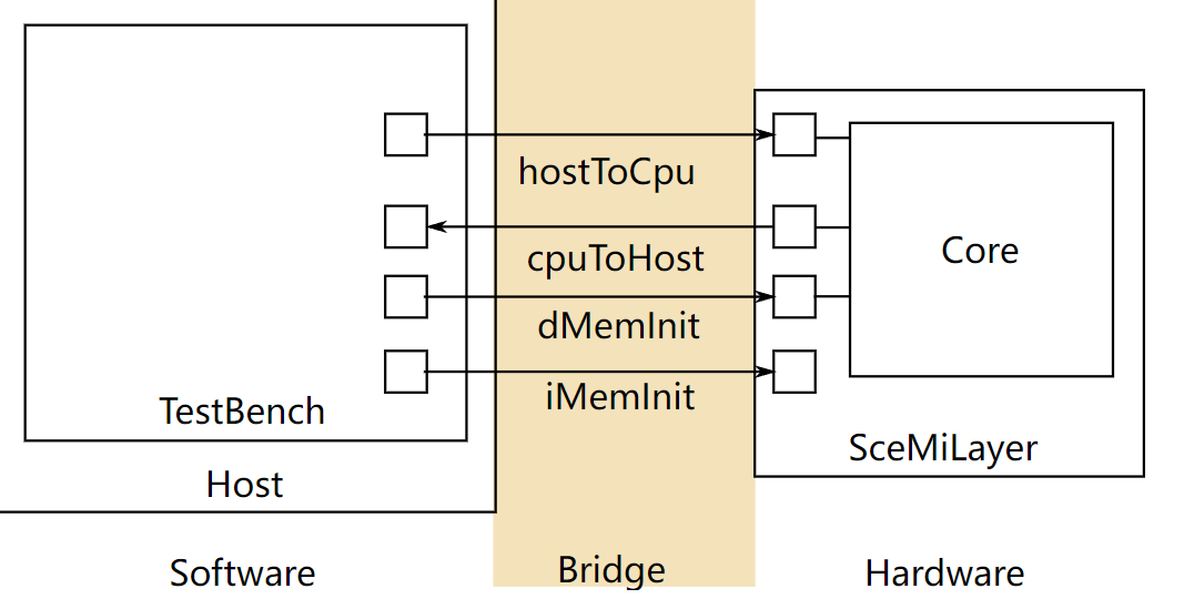
图 1 显示了本实验的 SceMi 设置。在设计和调试处理器时,我们经常需要另一个处理器的帮助,我们称之为宿主处理器(图 1 中标记为 "Host")。为了与宿主区分,我们
可以将你设计的处理器(图 1 中标记为 "Core")称为目标处理器。SceMiLayer 实例化来自指定处理器 BSV 文件的处理器和 SceMi 端口,用于处理器的 hostToCpu、cpuToHost、iMemInit 和 dMemInit 接口。SceMiLayer 还提供了一个 SceMi 端口,用于从测试台重置核心,允许在处理器上运行多个程序,而无需重新配置 FPGA。
由于我们只在本实验中在仿真中运行处理器,我们将绕过通过 iMemInit 和 dMemInit 接口初始化内存的耗时阶段。相反,我们将在仿真开始时直接使用内存初始化文件(.vmh 文件,介绍在编译汇编测试和基准测试中)加载内存所需的值,并将为每个程序重新启动仿真。
SceMiLayer 和 Bridge 的源代码位于 scemi/ 目录中。SceMi 链接在仿真时使用 TCP 桥,在实际 FPGA 上运行时使用 PCIe 桥。
构建项目
文件 scemi/sim/project.bld 描述了如何使用 build 命令构建项目,该命令是 Bluespec 安装的一部分。运行
build --doc
以获取有关 build 命令的更多信息。可以通过在 scemi/sim/ 目录中运行以下命令从头开始重新构建整个项目,其中 <proc_name> 是本实验指南中指定的处理器名称之一。这将覆盖之前通过 build 调用生成的可执行文件。
旁注:单独运行
build -v会打印一个错误消息,其中包含所有有效的处理器名称。
编译汇编测试和基准测试
我们的 SceMi 测试台运行指定为 Verilog Memory Hex (vmh) 格式的 RISC-V 程序。programs/assembly 目录包含汇编测试的源代码,而 programs/benchmarks 目录包含基准程序的源代码。我们将使用这些程序来测试处理器的正确性和性能。每个目录下都提供了一个 Makefile,用于生成 .vmh 格式的程序。
要编译所有汇编测试,请转到 programs/assembly 目录并运行 make。这将创建一个名为 programs/build/assembly 的新目录,其中包含所有汇编测试的编译结果。其下的 vmh 子目录包含所有的 .vmh 文件,而 dump 子目录包含所有转储的汇编代码。如果您忘记了这样做,将会看到以下错误消息:
-- assembly test: simple --
ERROR: ../../programs/build/assembly/vmh/simple.riscv.vmh does not exit, you need to first compile
同样,转到 programs/benchmarks 直接运行 make 命令来编译所有基准测试。编译结果将位于 programs/build/benchmarks 目录中。
现在编译汇编测试和基准测试。RISC-V 工具链应该能在所有 vlsifarm 机器上运行,但可能不适用于普通的 Athena 集群机器。我们建议您至少最初在 vlsifarm 机器上编译这些程序,然后,您可以使用普通的 Athena 集群机器来完成本实验。
programs/build/assembly/vmh 目录中的 .vmh 文件是汇编测试,它们如下介绍:
| 文件名 | 内容 |
|---|---|
simple.riscv.vmh | 包含汇编测试的 |
基本基础代码,并运行 100 条 NOP 指令("NOP" 代表 "无操作")。 |
| bpred_bht.riscv.vmh | 包含许多分支历史表可以很好预测的分支。 |
| bpred_j.riscv.vmh | 包含许多跳转指令,分支目标缓冲区可以很好地预测。 |
| bpred_ras.riscv.vmh | 包含许多通过寄存器进行的跳转,返回地址栈可以很好地预测。 |
| cache.riscv.vmh | 通过对别名在较小内存中的地址进行读写来测试缓存。 |
| <inst>.riscv.vmh | 测试特定指令。 |
每个汇编测试都会打印周期计数、指令计数和测试是否通过。simple.riscv.vmh 在单周期处理器上的示例输出为
102
103
PASSED
第一行是周期计数,第二行是指令计数,最后一行显示测试通过。指令计数比周期计数大,因为我们在读取周期计数 CSR(cycle)后读取指令计数 CSR(instret)。如果测试失败,最后一行将是
FAILED exit code = <failure code>
可以使用失败代码通过查看汇编测试的源代码来定位问题。
我们强烈建议在对处理器进行任何更改后重新运行所有汇编测试,以验证您没有破坏任何内容。当试图定位错误时,运行汇编测试将缩小问题指令的可能性。
programs/build/benchmarks/ 中的基准测试评估处理器的性能。这些基准测试简要介绍如下:
| 文件名 | 功能 |
|---|---|
median.riscv.vmh | 一维三元素中值过滤器。 |
multiply.riscv.vmh | 软件乘法。 |
qsort.riscv.vmh | 快速排序。 |
towers.riscv.vmh | 汉诺塔。 |
vvadd.riscv.vmh | 向量-向量加法。 |
每个基准测试都会打印其名称、周期计数、指令计数、返回值以及是否通过。单周期处理器上中值基准测试的示例输出为
Benchmark median
Cycles = 4014
Insts  = 4015
Return 0
PASSED
如果基准测试通过,最后两行应为 Return 0 和 PASSED。如果基准测试失败,最后一行将是
FAILED exit code = <failure code>
性能以每周期指令数 (IPC) 衡量,我们通常希望提高 IPC。对于我们的流水线,IPC 永远不会超过 1,但我们应该能够通过良好的分支预测器和适当的旁路接近它。
使用测试台
我们的 SceMi 测试台是在宿主处理器上运行的软件,通过 SceMi 链接与 RISC-V 处理器交互,如图 1 所示。测试台启动处理器并处理 toHost 请求,直到处理器表明已成功或未成功完成。例如,测试输出中的周期计数实际上是处理器发出的 toHost 请求,请求打印一个整数,测试台通过打印该整数来处理这些请求。测试输出的最后一行(即 PASSED 或 FAILED)也是由测试台根据指示处理完成的 toHost 请求打印出来的。
要运行测试台,请首先按照[构建项目](http://csg.csail.mit.edu
/6.175/archive/2016/labs/lab5-riscv-intro.html#build)中的描述构建项目,并按照编译汇编测试和基准测试中的描述编译 RISC-V 程序。对于仿真,将创建可执行文件 bsim_dut,在启动测试台时应运行此文件。在仿真中,我们的 RISC-V 处理器总是加载文件 scemi/sim/mem.vmh 来初始化(数据)内存。因此,我们只需要复制我们想要运行的测试程序的 .vmh 文件(对应于指令内存)即可。
例如,要在仿真中在处理器上运行中值基准测试,你可以在 scemi/sim 目录下使用以下命令:
cp ../../programs/build/benchmarks/vmh/median.riscv.vmh mem.vmh
./bsim_dut > median.out &
./tb
为方便起见,我们在 scemi/sim 目录中提供了脚本 run_asm.sh 和 run_bmarks.sh,分别运行所有汇编测试和基准测试。bsim_dut 的标准输出(stdout)将重定向到 logs/<test name>.log 文件。
测试台输出
RISC-V 仿真有两个输出来源。这些包括 BSV $display 语句(包括消息和错误)和 RISC-V 打印语句。
BSV $display 语句由 bsim_dut 打印到 stdout。BSV 还可以使用 $fwrite(stderr, ...) 语句将内容打印到标准错误(stderr)。run_asm.sh 和 run_bmarks.sh 脚本将 bsim_dut 的 stdout 重定向到 logs/<test name>.log 文件。
RISC-V 打印语句(例如,programs/benchmarks/common/syscall.c 中的 printChar、printStr 和 printInt 函数)通过将字符和整数移至 mtohost CSR 来处理。测试台从 cpuToHost 接口读取,并在接收到字符和整数时将它们打印到 stderr。
练习 0(0 分): 通过转到
programs/assembly和programs/benchmarks目录并运行make编译测试程序。在scemi/sim目录中编译单周期 RISC-V 实现并通过以下命令测试它:$ build -v onecycle $ ./run_asm.sh $ ./run_bmarks.sh在编译 BSV 代码(即
build -v onecycle)期间,你可能会看到许多警告,出现在 "code generation for mkBridge starts" 之后。这些警告针对的是 SceMi 基础设施,通常你不需要关心它们。
实用提示: 在
scemi/sim目录中运行$ ./clean将删除使用
build构建的任何文件。
应对 AFS 超时问题
在运行构建工具时,AFS 超时错误可能如下所示:
   ...
code generation for mkBypassRFile starts
Error: Unknown position: (S0031)
  Could not write the file `bdir_dut/mkBypassRFile.ba':
    timeout
tee: ./onecycle_compile_for_bluesim.log: Connection timed out
!!! Stage compile_for_bluesim command encountered an error -- aborting build.
!!! Look in the log file at ./onecycle_compile_for_bluesim.log for more information.
由于各种原因,AFS 可能会超时,导致你的 Bluespec 构建失败。我们可以将构建目录移到 AFS 之外的位置,这可以缓解这个问题。首先,在 /tmp 中创建一个目
录:
mkdir /tmp/<your_user_name>-lab5
然后,打开 scemi/sim/project.bld,你会发现以下行:
[common]
hide-target
top-module:             mkBridge
top-file:               ../Bridge.bsv
bsv-source-directories: ../../scemi ../../src ../../src/includes
verilog-directory:      vlog_dut
binary-directory:       bdir_dut
simulation-directory:   simdir_dut
info-directory:         info_dut
altera-directory:       quartus
xilinx-directory:       xilinx
scemi-parameters-file:  scemi.params
将 verilog-directory、binary-directory、simulation-directory 和 info-directory 更改为包含新的临时目录。例如,如果你的用户名是 "alice",你的新文件夹将是:
verilog-directory:      /tmp/alice-lab5/vlog_dut
binary-directory:       /tmp/alice-lab5/bdir_dut
simulation-directory:   /tmp/alice-lab5/simdir_dut
info-directory:         /tmp/alice-lab5/info_dut
完成本实验后,请记得删除你的 tmp 目录。如果你忘记了哪个临时目录是你的,查看 project.bld 或使用 ls -l 找到带有你的用户名的那个。
多周期 RISC-V 实现
提供的代码 src/OneCycle.bsv 实现了一个单周期哈佛架构 RISC-V 处理器。(哈佛架构具有独立的指令和数据存储器。)这个处理器能够在一个周期内完成操作,因为它具有独立的指令和数据存储器,且每个存储器在同一周期内对加载给出响应。在本实验的这一部分,你将制作两种不同的多周期实现,这些实现是由更现实的内存结构危害驱动的。
两周期冯·诺依曼架构 RISC-V 实现
哈佛架构的一种替代方案是冯·诺依曼架构。(冯·诺依曼架构也称为普林斯顿架构。)冯·诺依曼架构将指令和数据存储在同一内存中。如果只有一个内存同时保存指令和数据,则存在结构危害(假设内存不能在同一周期内被访问两次)。要解决这个危害,你可以将处理器分成两个周期:指令取取 和 执行。
- 在指令取取阶段,处理器从内存中读取当前指令并对其进行解码。
- 在执行阶段,处理器读取寄存器文件、执行指令、进行 ALU 操作、进行内存操作,并将结果写入寄存器文件。
创建两周期实现时,你将需要一个寄存器来在两个阶段间保持中间数据,以及一个状态寄存器来跟踪当前状态。中间数据寄存器将在指令取取期间被写入,在执行期间被读取。状态寄存器将在指令取取和执行之间切换。为了简化操作,你可以使用提供的 Stage 类型定义作为状态寄存器的类型。
练习 1(15 分): 在
TwoCycle.bsv中实现一个两周期 RISC-V 处理器,使用单一内存来存储指令和数据。已为你提供了单一内存模块mem供使用。通过转到scemi/sim目录并使用以下命令测试此处理器:$ build -v twocycle $ ./run_asm.sh $ ./run_bmarks.sh
四周期 RISC-V 实现,支持内存延迟
一周期和两周期 RISC-V 处理器假设内存具有组合读取功能;即如果你设置读取地址,那么读取的数据将在同一时钟周期内有效。大多数内存的读取具有更长的延迟:首先你设置地址位,然后在下一个时钟周期中读取结果才准备好。如果我们将之前 RISC-V 处理器实现中的内存更改为具有读取延迟的内存,那么我们将引入另一个结构危害:读取的结果不能在执行读取的同一周期中使用。这种结构危害可以通过将处理器进一步分成四个周期来避免:指令取取、指令解码、执行 和 写回。
- 指令取取阶段,如前所述,将地址线设置在内存的
PC上以读取当前指令。 - 指令解码阶段从内存获取指令、解码并读取寄存器。
- 执行阶段进行 ALU 操作,为存储指令写入数据到内存,并为读取指令设置内存地址线。
- 写回阶段从 ALU 获取结果或从内存读取结果(如果有的话)并写入寄存器文件。
这种处理器将需要更多的阶段间寄存器和扩展的状态寄存器。你可以使用修改过的 Stage 类型定义作为状态寄存器的类型。
由 mkDelayedMemory 实现的一周期读取延迟内存。此模块具有一个接口 DelayedMemory,该接口将内存请求和内存响应分离。请求仍以使用 req 方法的相同方式进行,但此方法不再同时返回响应。为了获取上一次读取请求的结果,你必须在稍后的时钟周期中调用 resp 动作值方法。存储请求不会生成任何响应,因此你不应为存储调用 resp 方法。更多细节可以在 src/includes 中的源文件 DelayedMemory.bsv 中找到。
练习 2(15 分):
如上所述,在
FourCycle.bsv中实现一个四周期 RISC-V 处理器。使用已包含在FourCycle.bsv中的延迟内存模块mem作为指令和数据内存。使用以下命令测试此处理器:$ build -v fourcycle $ ./run_asm.sh $ ./run_bmarks.sh
两阶段流水线 RISC-V 实现
虽然两周期和四周期实现允许处理器处理某些结构危害,但它们的性能并不理想。今天的所有处理器都是流水线化的,以提高性能,它们通常具有重复的硬件来避免诸如两周期和四周期 RISC-V 实现中所见的内存危害之类的结构危害。流水线引入了更多的数据和控制危害,处理器必须处理。为了避免数据危害,我们现在只研究两阶段流水线。
两阶段流水线使用两周期实现将工作分成两个阶段的方式,并使用独立的指令和数据内存并行运行这些阶段。这意味着当一条指令正在执行时,下一条指令正在被取出。对于分支指令,下一条指令并不总是已知的。这被称为控制危害。
为了处理这种控制危害,请在取指阶段使用 PC+4 预测器,并在分支错误预测发生
时纠正 PC。ExecInst 的 mispredict 字段在此处将非常有用。
练习 3(30 分):
在
TwoStage.bsv中实现一个两周期流水线 RISC-V 处理器,使用独立的指令和数据内存(具有组合读取功能,就像OneCycle.bsv中的内存一样)。你可以实现非弹性或弹性流水线。使用以下命令测试此处理器:$ build -v twostage $ ./run_asm.sh $ ./run_bmarks.sh
每周期指令数(IPC)
处理器性能通常以每周期指令数 (IPC) 衡量。这个指标是吞吐量的度量,即平均每周期完成的指令数。要计算 IPC,请将完成的指令数除以完成它们所需的周期数。单周期实现的 IPC 为 1.0,但它将不可避免地需要一个长的时钟周期来考虑传播延迟。结果,我们的单周期处理器并不像听起来那么快。两周期和四周期实现分别达到 0.5 和 0.25 的 IPC。
流水线实现的处理器将实现 0.5 到 1.0 IPC 之间的某处。分支错误预测会降低处理器的 IPC,因此你的 PC+4 下一地址预测器的准确性对于拥有高 IPC 的处理器至关重要。
讨论问题 1(5 分): 对于
run_bmarks.sh脚本测试的每个基准测试,两阶段流水线处理器的 IPC 是多少?
讨论问题 2(5 分): 从 IPC 计算下一地址预测器准确性的公式是什么?(提示,当 PC+4 预测正确时,执行一条指令需要多少周期?当预测错误时呢?)使用这个公式,每个基准测试的 PC+4 下一地址预测器的准确性是多少?
下一地址预测
现在,让我们使用更高级的下一地址预测器。其中一个例子是分支目标缓冲区 (BTB)。它根据当前的程序计数器 (PC) 的值预测要取出的下一条指令的位置。对于绝大多数指令来说,这个地址是 PC + 4(假设所有指令都是 4 字节)。但是,对于跳转和分支指令来说,情况并非如此。因此,BTB 包含了之前使用过的不仅仅是 PC+4 的下一个地址(“分支目标”)的表,以及生成这些分支目标的 PC。
Btb.bsv 包含了一个 BTB 的实现。其接口有两个方法:predPc 和 update。方法 predPc 接受当前 PC 并返回一个预测。方法 update 接受一个程序计数器和该程序计数器的指令的下一个地址,并将其添加为预测(如果不是 PC+4 的话)。
应当调用 predPc 方法来预测下一个 PC,而在分支解析后应调用 update 方法。执行阶段需要当前指令的 PC 和预测的 PC 来解析分支,因此你需要在流水线寄存器或 FIFO 中存储这些信息。
ExecInst 的 mispredict 和 addr 字段在这里将非常有用。需要注意的是,addr 字段并不总是下一条指令的正确 PC——它将是内存加载和存储的地址。我们可以进行高级推理,得出加载和存储从不出现错误的下一 PC 预
测,或者我们可以在执行阶段检查指令类型以得出下一 PC。
练习 4(10 分): 在
TwoStageBTB.bsv中,为你的两周期流水线 RISC-V 处理器添加一个 BTB。BTB 模块已在给定代码中实例化。使用以下命令测试此处理器:$ build -v twostagebtb $ ./run_asm.sh $ ./run_bmarks.sh
讨论问题 3(5 分): 使用 BTB 的两阶段流水线处理器的 IPC 是多少,对于
run_bmarks.sh脚本测试的每个基准测试而言,它有多大改进?
讨论问题 4(5 分): 添加 BTB 如何改变
bpred_*微基准测试的性能?(提示:bpred_j的周期数应该减少。)
讨论问题 5(可选): 完成这个实验你花了多长时间?
完成后记得使用 git push 推送你的代码。
额外讨论问题
讨论问题 6(5 额外分): 查看
bpred_*基准测试的汇编源代码并解释为什么每个基准测试改进、保持不变或变得更糟。
讨论问题 7(5 额外分): 你会如何改进 BTB 以改善
bpred_bht的结果?
© 2016 麻省理工学院。保留所有权利。
实验 6: 具有六阶段流水线和分支预测的 RISC-V 处理器
实验 6截止日期: 2016年11月7日,美东时间晚上11:59:59。
本实验的交付物为:
- 在
SixStage.bsv、Bht.bsv和SixStageBHT.bsv中完成的练习1至4的答案- 在
discussion.txt中完成的讨论问题1至9的答案
引言
本实验是你对现实中的 RISC-V 流水线和分支预测的介绍。在本实验结束时,你将拥有一个具有多种地址和分支预测器协同工作的六级 RISC-V 流水线。
注意:在本实验中,我们使用一位全局时期(而非无限分布时期)来终止错误路径指令。请学习全局时期的幻灯片:[pptx] [pdf],以理解全局时期方案。幻灯片的内容也将在教程中讲解。
实验设施的新增部分
新包含的文件
以下文件出现在 src/includes/ 中:
| 文件名 | 描述 |
|---|---|
FPGAMemory.bsv | FPGA上常见的块 RAM 的封装器。它的接口与上一个实验中的 DelayedMemory 相同。 |
SFifo.bsv | 三种可搜索的 FIFO 实现:基于流水线 FIFO、基于旁路 FIFO 和基于无冲突 FIFO 的实现。所有实现都假设在 enq 之前立即完成搜索。 |
Scoreboard.bsv | 基于可搜索 FIFO 的三种记分牌实现。流水线记分牌使用流水线可搜索 FIFO,旁路记分牌使用旁路可搜索 FIFO,无冲突记分牌使用无冲突可搜索 FIFO。 |
Bht.bsv | 一个空文件,在其中你将实现一个分支历史表(BHT)。 |
新的汇编测试
以下文件出现在 programs/assembly/src 中:
| 文件名 | 描述 |
|---|---|
bpred_j_noloop.S | 与 bpred_j.S 类似的汇编测试,但移除了外部循环。 |
新的源文件
以下文件出现在 src/ 中:
| 文件名 | 描述 |
|---|---|
TwoStage.bsv | 包含一个两级流水线的 RISC-V 处理器的初始文件。此处理器使用 BTB 进行地址预测。使用 twostage 目标编译。 |
SixStage.bsv | 一个空文件,在其中你将把两级流水线扩展为六级流水线。使用 sixstage 目标编译。 |
SixStageBHT.bsv | 一个空文件,在其中你将把分支历史表(BHT)整合到六级流水线中。使用 sixstagebht 目标编译。 |
SixStageBonus.bsv | 一个空文件,在其中你可以改进前一个处理器以获得额外学分。使用 sixstagebonus 目标编译。 |
测试改进
在前一个实验中,使用命令 build -v <proc_name>(从 scemi/sim/ 目录运行)用于构建 bsim_dut 和 tb。在本实验中,此命令构建 <proc_name>_dut 而非 `
bsim_dut`,因此切换处理器类型时不会删除其他处理器构建。
模拟脚本现在要求您指定目标处理器:
./run_asm.sh <proc_name>
./run_bmarks.sh <proc_name>
模拟单个测试要求您运行正确的模拟可执行文件:
cp ../../programs/build/{assembly,benchmarks}/vmh/<test_name>.riscv.vmh mem.vmh
./<proc_name>_dut > out.txt &
./tb
两级流水线:TwoStage.bsv
TwoStage.bsv 包含一个两级流水线的 RISC-V 处理器。这个处理器与你在上一个实验中构建的处理器不同,因为它在第一阶段读取寄存器值,存在数据危害。
讨论问题 1(10 分): 调试实践!
如果你将 BTB 替换为简单的
pc + 4地址预测,处理器仍然可以工作,但性能不佳。如果你用一个非常糟糕的预测器替换它,该预测器预测每个pc的下一个指令是pc,它应该仍然可以工作,但性能会更差,因为每个指令都需要重定向(除非指令回到其自身)。如果你真的将预测设置为pc,你会在汇编测试中得到错误;第一个错误将来自于cache.riscv.vmh。
- 你得到的错误是什么?
- 处理器中发生了什么导致这种情况?
- 为什么你在 PC+4 和 BTB 预测器中没有得到这个错误?
- 你将如何修复它?
你实际上不必修复这个错误,只需回答问题。(提示:查看
ExecInst结构的addr字段。)
六级流水线:SixStage.bsv
六级流水线应该分为以下阶段:
- 指令取回 —— 从 iMem 请求指令并更新 PC
- 解码 —— 接收来自 iMem 的响应并解码指令
- 寄存器取值 —— 从寄存器文件读取
- 执行 —— 执行指令并在必要时重定向处理器
- 内存 —— 向 dMem 发送内存请求
- 写回 —— 接收来自 dMem 的内存响应(如果适用)并写入寄存器文件
应将 IMemory 和 DMemory 实例替换为 FPGAMemory 实例,以便在 FPGA 上实现。
练习 1(20 分):从
TwoStage.bsv中的两级实现开始,将每个内存替换为FPGAMemory并在SixStage.bsv中扩展为六级流水线。在模拟中,基准测试qsort可能需要更长时间(助教的桌面上为21秒,vlsifarm 机器上可能需要更长时间)。
注意,两级实现使用无冲突寄存器文件和记分牌。然而,你可以使用流水线或旁路版本的这些组件以获得更好的性能。同样,你可能想改变记分牌的大小。
讨论问题 2(5 分):你有什么证据表明所有流水线阶段可以在同一个周期内触发?
讨论问题 3(5 分):在你的六级流水线处理器中,纠正错误预测的指令需要多少个周期?
讨论问题 4(5 分):如果一条指令依赖于流水线中紧接其前的指令的结果,这条指令会延迟多少个周期?
讨论问题 5(5 分):你为每个基准测试获得了多少 IPC?
添加分支历史表:SixStageBHT.bsv
分支历史表(BHT)是一个跟踪分支历史的结构,用于方向预测。你的 BHT 应该使用从程序计数器(PC)中取得的参数化位数作为索引——通常是从第 n+1 位到第 2 位,因为第 1 和 0 位总是零。每个索引应该有一个两位的饱和计数器。不要在 BHT 中包含任何有效位或标签;我们不关心我们的预测中的别名问题。
练习 2(20 分):在
Bht.bsv中实现一个使用参数化位数作为表索引的分支历史表。
讨论问题 6(10 分):规划!
这个实验中最困难的事情之一是正确地训练和整合 BHT 到流水线中。在仍然看到不错的结果的情况下,可以犯很多错误。通过基于方向预测的基础知识制定一个好的计划,你将避免许多这些错误。
对于这个讨论问题,说明你将 BHT 整合到流水线中的计划。以下问题应该有助于指导你:
BHT 将被放置在流水线的哪个位置?
哪个流水线阶段执行对 BHT 的查找?
在哪个流水线阶段将使用 BHT 预测?
BHT 预测是否需要在流水线阶段之间传递?
如何使用 BHT 预测重定向 PC?
你需要添加新的 epoch 吗? >
如何处理重定向消息?
如果重定向,你需要改变当前指令及其数据结构吗?
你将如何训练 BHT?
哪个阶段产生 BHT 的训练数据?
哪个阶段将使用接口方法来训练 BHT?
如何发送训练数据?
你将为哪些指令训练 BHT?
你如何知道你的 BHT 是否有效?
练习 3(20 分):将 256 个条目(8 位索引)的 BHT 集成到
SixStage.bsv的六级流水线中,并将结果放入SixStageBHT.bsv中。
讨论问题 7(5 分):与
SixStage.bsv处理器相比,你在bpred_bht.riscv.vmh测试中看到了多少提升?
练习 4(10 分):将 JAL 指令的地址计算上移到解码阶段,并使用 BHT 重定向逻辑来重定向这些指令。
讨论问题 8(5 分):与
SixStage.bsv处理器相比,你在bpred_j.riscv.vmh和bpred_j_noloop.riscv.vmh测试中看到了多少提升?
讨论问题 9(5 分):你在每个基准测试中获得了多少 IPC?与原始六级流水线相比,这有多大提升?
讨论问题 10(选做):完成这个实验室你用了多长时间?
完成后记得使用 git push 将你的代码推送。
额外改进:SixStageBonus.bsv
这一节探讨了两种加速间接跳转到寄存器中存储的地址的方法(JALR)。
练习 5(10 附加分):JALR 指令在寄存器取值阶段已知目标地址。在寄存器取值阶段为 JALR 指令添加一个重定向路径,并将结果放入
SixStageBonus.bsv中。bpred_ras.riscv.vmh测试应该会有稍微更好的结果,有了这种改进。
大多数程序中找到的 JALR 指令被用作从函数调用返回。这意味着这种返回的目标地址是由先前的 JAL 或 JALR 指令写入返回地址寄存器 x1(也称为 ra)的,该指令启动了函数调用。
为了更好地预测 JALR 指令,我们可以在处理器中引入返回地址堆栈(RAS)。根据 RISC-V ISA,使用 rd=x0 和 rs1=x1 的 JALR 指令通常用作函数调用的返回指令。此外,使用 rd=x1 的 JAL 或 JALR 指令通常用作跳转以启动函数调用。因此,我们应该为带有 rd=x1 的 JAL/JALR 指令推送 RAS,并为带有 rd=x0 和 rs1=x1 的 JALR 指令弹出 RAS。
练习 6(10 附加分):实现一个返回地址堆栈,并将其集成到处理器的解码阶段(
SixStageBonus.bsv)。8 个元素的堆栈应该足够。如果堆栈满了,你可以简单地丢弃最旧的数据。bpred_ras.riscv.vmh测试应该会有更好的结果,有了这种改进。如果你在一个单独的 BSV 文件中实现了 RAS,请确保将其添加到 git 仓库中进行评分。
© 2016 麻省理工学院。保留所有权利。
实验 7: 带有 DRAM 和缓存的 RISC-V 处理器
实验 7截止日期: 2016年11月18日,美东时间晚上11:59:59。
你需要提交的实验 7内容包括:
- 在
WithoutCache.bsv和WithCache.bsv中完成练习 1、2 和 4 的答案- 在
discussion.txt中完成讨论问题 1 到 3 的答案
简介
现在,你已经拥有了一个具有分支目标和方向预测器(BTB 和 BHT)的六级流水线 RISC-V 处理器。不幸的是,你的处理器只能运行能够适应 256 KB FPGA块 RAM 的程序。这对于我们运行的小型基准程序(如250项快速排序)来说是足够的,但大多数有趣的应用程序都远大于 256 KB。幸运的是,我们使用的 FPGA 板配备了 1 GB DDR3 DRAM,可供 FPGA 访问。这非常适合存储大型程序,但由于 DRAM 读取延迟相对较长,这可能会影响性能。
本实验将重点使用 DRAM 而非块 RAM 作为主程序和数据存储来存储更大的程序,并添加缓存以减少长延迟 DRAM 读取对性能的影响。
首先,你将编写一个转换模块,将 CPU 内存请求转换为 DRAM 请求。此模块大大扩展了你的程序存储空间,但由于几乎每个周期都要从 DRAM 读取,你的程序将运行得更慢。接下来,你将实现一个缓存来减少需要从 DRAM 读取的次数,从而提高处理器性能。最后,你将为 FPGA 合成你的设计,并运行需要 DRAM 和长时间运行的非常大的基准测试。
测试基础设施的变化
如果我们每次运行一个新测试就必须重新配置 FPGA,那么运行所有的组装测试将需要很长时间(重新配置 FPGA 大约需要一分钟)。由于我们没有更改硬件,我们将只配置一次 FPGA,然后每次想要运行新测试时进行软重置。软件测试台(位于 scemi/Tb.cpp)将启动软重置,将 *.vmh 文件写入您的 FPGA 的 DRAM,并启动新测试。在每个测试开始之前,软件测试台还会打印出基准测试的名称,以帮助调试。在软件仿真(无 FPGA)中,我们还将模拟将 *.vmh 文件写入 DRAM 的过程,因此仿真时间也会比以前更长。
以下是使用名为 withoutcache 的处理器来仿真 simple.S 和 add.S 组装测试的示例命令:
cd scemi/sim
./withoutcache_dut > log.txt &
./tb ../../programs/build/assembly/vmh/simple.riscv.vmh ../../programs/build/assembly/vmh/add.riscv.vmh
这是样本输出:
---- ../../programs/build/assembly/vmh/simple.riscv.vmh ----
1196
103
通过

---- ../../programs/build/assembly/vmh/add.riscv.vmh ----
5635
427
通过

SceMi 服务线程完成!
我们还提供了两个脚本 run_asm.sh 和 run_bmarks.sh 来分别运行所有组装测试和基准测试。例如,我们可以使用以下命令测试处理器 withoutcache:
./run_asm.sh withoutcache
./run_bmarks.sh withoutcache
BSV 的标准输出将分别重定向到 asm.log 和 bmarks.log。
DRAM 接口
你将在本课程中使用的 VC707 FPGA 板配备了 1 GB DDR3 DRAM。DDR3 内存具有 64 位宽的数据总线,但每次传输都会发送八个 64 位块,因此实际上它的作用就像一个 512 位宽的内存。DDR3 内存具有高吞吐量,但其读取延迟也比较高。
Sce-Mi 接口为我们生成了 DDR3 控制器,我们可以通过 MemoryClient 接口连接到它。本实验中为你提供的 typedef 使用了 BSV 的内存包中的类型(见 BSV 参考指南或 $BLUESPECDIR/BSVSource/Misc/Memory.bsv 的源代码)。以下是 src/includes/MemTypes.bsv 中与 DDR3 内存相关的一些 typedef:
typedef 24 DDR3AddrSize;
typedef Bit#(DDR3AddrSize) DDR3Addr;
typedef 512 DDR3DataSize;
typedef Bit#(DDR3DataSize) DDR3Data;
typedef TDiv#(DDR3DataSize, 8) DDR3DataBytes;
typedef Bit#(DDR3DataBytes) DDR3ByteEn;
typedef TDiv#(DDR3DataSize, DataSize) DDR3DataWords;

// 下面的 typedef 等同于:
// typedef struct {
//     Bool        write;
//     Bit#(64)    byteen;
//     Bit#(24)    address;
//     Bit#(512)   data;
// } DDR3_Req deriving (Bits, Eq);
typedef MemoryRequest#(DDR3AddrSize, DDR3DataSize) DDR3_Req;

// 下面的 typedef 等同于:
// typedef struct {
//     Bit#(512)   data;
// } DDR3_Resp deriving (Bits, Eq);
typedef MemoryResponse#(DDR3DataSize) DDR3_Resp;

// 下面的 typedef 等同于:
// interface DDR3_Client;
//     interface Get#( DDR3_Req )  request;
//     interface Put#( DDR3_Resp ) response;
// endinterface;
typedef MemoryClient#(DDR3AddrSize, DDR3DataSize) DDR3_Client;
DDR3_Req
对 DDR3 的读取和写入请求与对 FPGAMemory 的请求不同。最大的区别是字节启用信号 byteen。
write—— 布尔值,指定此请求是写入请求还是读取请求。byteen—— 字节启用,指定将写入哪些 8 位字节。此字段对于读取请求无效。如果你想写入所有 16 字节(即 512 位),你将需要将此设置为全部为 1。你可以使用文字'1(注意单引号)或maxBound来实现。address—— 读取或写入请求的地址。DDR3 内存以 512 位块为单位进行寻址,因此地址 0 指的是第一个 512 位块,地址 1 指的是第二个 512 位块。这与 RISC-V 处理器使用的字节寻址非常不同。data—— 用于写入请求的数据值。
DDR3_Resp
DDR3 内存只对读取发送响应,就像 FPGAMemory 一样。内存响应类型是一种结构体——因此,你将不会直接接收到 Bit#(512) 值,而必须访问响应中的 data 字段以获取 Bit#(512) 值。
DDR3_Client
DDR3_Client 接口由一个 Get 子接口和一个 Put 子接口组成。这个接口由处理器公开,Sce-Mi 基础设施将其连接到 DDR3 控制器。你无需担心构建此接口,因为示例代码中已为你完成。
示例代码
这里是一些展示如何构建 FIFOs 以及 DDR3 内存接口初始化接口的示例代码,
此示例代码提供在 src/DDR3Example.bsv 中。
import GetPut::*;
import ClientServer::*;
import Memory::*;
import CacheTypes::*;
import WideMemInit::*;
import MemUtil::*;
import Vector::*;

// 其他包和类型定义

(* synthesize *)
module mkProc(Proc);
 Ehr#(2, Addr)  pcReg <- mkEhr(?);
 CsrFile         csrf <- mkCsrFile;

 // 其他处理器状态和组件

 // 接口 FIFO 到真实的 DDR3
 Fifo#(2, DDR3_Req)  ddr3ReqFifo  <- mkCFFifo;
 Fifo#(2, DDR3_Resp) ddr3RespFifo <- mkCFFifo;
 // 初始化 DDR3 的模块
 WideMemInitIfc       ddr3InitIfc <- mkWideMemInitDDR3( ddr3ReqFifo );
 Bool memReady = ddr3InitIfc.done;

 // 将 DDR3 包装成 WideMem 接口
 WideMem           wideMemWrapper <- mkWideMemFromDDR3( ddr3ReqFifo, ddr3RespFifo );
 // 将 WideMem 接口分割为两个(多路复用方式使用)
 // 这个分割器只在重置后生效(即 memReady && csrf.started)
 // 否则 guard 可能失败,我们将获取到垃圾 DDR3 响应
 Vector#(2, WideMem)     wideMems <- mkSplitWideMem( memReady && csrf.started, wideMemWrapper );
 // 指令缓存应使用 wideMems[1]
 // 数据缓存应使用 wideMems[0]

 // 在软重置期间,一些垃圾可能进入 ddr3RespFifo
 // 这条规则将排空所有此类垃圾
 rule drainMemResponses( !csrf.started );
  ddr3RespFifo.deq;
 endrule

 // 其他规则

 method ActionValue#(CpuToHostData) cpuToHost if(csrf.started);
  let ret <- csrf.cpuToHost;
  return ret;
 endmethod

 // 将 ddr3RespFifo empty 添加到 guard 中,确保垃圾已被排空
 method Action hostToCpu(Bit#(32) startpc) if ( !csrf.started && memReady && !ddr3RespFifo.notEmpty );
  csrf.start(0); // 只有 1 个核心,id = 0
  pcReg[0] <= startpc;
 endmethod

 // 为测试台提供 DDR3 初始化的接口
 interface WideMemInitIfc memInit = ddr3InitIfc;
 // 接口到真实 DDR3 控制器
 interface DDR3_Client ddr3client = toGPClient( ddr3ReqFifo, ddr3RespFifo );
endmodule
在上述示例代码中,ddr3ReqFifo 和 ddr3RespFifo 作为与真实 DDR3 DRAM 的接口。在仿真中,我们提供了一个名为 mkSimMem 的模块来模拟 DRAM,该模块在 scemi/SceMiLayer.bsv 中实例化。在 FPGA 合成中,DDR3 控制器在顶层模块 mkBridge 中实例化,位于 $BLUESPECDIR/board_support/bluenoc/bridges/Bridge_VIRTEX7_VC707_DDR3.bsv。还有一些胶合逻辑在 scemi/SceMiLayer.bsv 中。
在示例代码中,我们使用模块 mkWideMemFromDDR3 将 DDR3_Req 和 DDR3_Resp 类型转换为更友好的 WideMem 接口,该接口定义在 src/includes/CacheTypes.bsv 中。
共享 DRAM 接口
示例代码中仅暴露了单一的与 DRAM 的接口,但你有两个模块将使用它:指令缓存和数据缓存。如果它们都向 ddr3ReqFifo 发送请求,并且都从 ddr3RespFifo 获取响应,那么它们的响应可能会混淆。为了处理这个问题,你需要一个单独的 FIFO 来跟踪响应应当返回的顺序。每个加载请求都与一个入队到排序 FIFO 的操作配对,该操作指定谁应该获取响应。
为了简化这个过程,我们提供了模块 mkSplitWideMem 来将 DDR3 FIFOs 分割为两个 WideMem 接口。这个模块定义在 src/includes/MemUtils.bsv 中。为了防止 mkSplitWideMem 过早采取行动并显示出预期之外的行为,我们将其第一个参数设置为 memReady && csrf.started,以在处理器启动之前冻结它。这也可以避免与 DRAM 内容初始化发生调度冲突。
处理软重置问题
如前所述,你将在启动每个新测试前对处理器状态进行软重置。在软重置期间,由于某些跨时钟域问题,一些垃圾数据可能会入队到 ddr3RespFifo 中。为了处理这个问题,我们添加了 drainMemResponses 规则来排空垃圾数据,并在 hostToCpu 方法的保护条件中添加了检查 drainMemResponses 是否为空的条件。
建议:在每个管道阶段的规则中添加
csrf.started到 guard 中。这可以防止在处理器启动之前 DRAM 被访问。
从前一个实验室迁移代码
本实验室提供的代码非常相似,但存在一些差异需要注意。大多数差异都在提供的示例代码 src/DDR3Example.bsv 中显示。
修改的 Proc 接口
Proc 接口现在只有单一的内存初始化接口,以匹配统一的 DDR3 内存。此内存初始化接口的宽度已扩展到每次传输 512 位。这个新的初始化接口的类型是 WideMemInitIfc,在 src/includes/WideMemInit.bsv 中实现。
空文件
本实验室的两个处理器实现:src/WithoutCache.bsv 和 src/WithCache.bsv 最初是空的。你应该将代码从 SixStageBHT.bsv 或 SixStageBonus.bsv 复制过来作为这些处理器的起点。src/includes/Bht.bsv 也是空的,因此你还需要将前一个实验室的代码复制过来。
新文件
以下是在 src/includes 文件夹下提供的新文件概述:
| 文件名 | 描述 |
|---|---|
Cache.bsv | 一个空文件,你将在本实验室中实现缓存模块。 |
CacheTypes.bsv | 关于缓存的类型和接口定义的集合。 |
MemUtil.bsv | 关于 DDR3 和 WideMem 的有用模块和函数的集合。 |
SimMem.bsv | 在仿真中使用的 DDR3 内存。它有 10 个周期的流水线访问延迟,但额外的胶合逻辑可能会增加访问 DRAM 的总延迟。 |
WideMemInit.bsv | DDR3 初始化模块。 |
MemTypes.bsv 也有一些变化。
使用 DRAM 而不使用缓存的处理器 WithoutCache.bsv
练习 1 (10 分):在
Cache.bsv中实现一个名为mkTranslator的模块,它接受与 DDR3 内存相关的某些接口(例如WideMem),并返回一个Cache接口(见CacheTypes.bsv)。该模块不应进行任何缓存,只需从
MemReq到 DDR3 请求(如果使用WideMem接口,则为WideMemReq)以及从 DDR3 响应(如果使用WideMem接口,则为CacheLine)到MemResp的转换。这将需要一些内部存储来跟踪你从主存返回的缓存行中需要哪个字。将mkTranslator集成到文件WithoutCache.bsv中的六阶段管线中(即你不应再使用mkFPGAMemory)。你可以通过在scemi/sim/目录下运行以下命令来构建这个处理器:$ build -v withoutcache并通过运行以下命令来测试此处理器:
$ ./run_asm.sh withoutcache和
$ ./run_bmarks.sh withoutcache在
scemi/sim/目录下。
讨论问题 1 (5 分):记录
./run_bmarks.sh withoutcache的结果。你在每个基准测试中看到的 IPC 是多少?
使用带有缓存的 DRAM 的处理器 WithCache.bsv
通过使用模拟的 DRAM 运行基准测试,你应该已经注意到你的处理器速度大大减慢了。通过记住之前的 DRAM 加载到缓存中,你可以重新提升处理器的速度,正如课堂上所描述的那样。
练习 2 (20 分):实现一个名为
mkCache的模块作为直接映射缓存,仅在替换缓存行时写回,并且仅在写缺失时分配。该模块应接受一个
WideMem接口(或类似的东西)并暴露一个Cache接口。使用CacheTypes.bsv中的typedefs来定义你的缓存大小和Cache接口。你可以使用寄存器向量或寄存器文件来实现缓存中的数组,但寄存器向量更容易指定初始值。将此缓存集成到WithoutCache.bsv中的相同管线,并将其保存在WithCache.bsv中。你可以通过在scemi/sim/目录下运行以下命令来构建此处理器:$ build -v withcache并通过运行以下命令来测试此处理器:
$ ./run_asm.sh withcache和
$ ./run_bmarks.sh withcache在
scemi/sim/目录下。
讨论问题 2 (5 分):记录
./run_bmarks.sh withcache的结果。你在每个基准测试中看到的 IPC 是多少?
运行大型程序
通过添加对 DDR3 内存的支持,你的处理器现在可以运行比我们一直在使用的小基准测试更大的程序。不幸的是,这些大型程序需要更长的运行时间,在许多情况下,模拟完成需要太长时间。现在是尝试 FPGA 合成的好时机。通过在 FPGA 上实现你的处理器,由于设计在硬件而非软件中运行,你将能够更快地运行这些大型程序。
练习 3 (0 分,但你仍然应该做这个): 在为 FPGA 合成之前,让我们试试看一个在模拟中运行时间很长的程序。程序
./run_mandelbrot.sh运行一个基准测试,使用 1 和 0 打印曼德博集合的方形图像。运行此基准测试以查看它在实时中的运行速度有多慢。请不要等待此基准测试完成,可以使用 Ctrl-C 提前终止。
为 FPGA 合成
你可以通过进入 scemi/fpga_vc707 文件夹并执行以下命令开始为 WithCache.bsv 进行 FPGA 合成:
vivado_setup build -v
这个命令将需要很长时间(大约一小时)并消耗大量计算资源。你可能想选择一个负载较轻的 vlsifarm 服务器。你可以使用 w 查看有多少人登录,并可以使用 top 或 uptime 查看正在使用的资源。
一旦完成,你可以通过运行 ./submit_bitfile 命令将你的 FPGA 设计提交给共享的 FPGA 板进行测试,并可以使用 ./get_results 检查结果。get_results 脚本将在你的结果准备好之前持续显示当前的 FPGA 状态。在 FPGA 上执行可能需要几分钟时间,如果其他学生也提交了作业,则可能需要更长时间。FPGA 上的 *.vmh 程序文件位于 /mit/6.175/fpga-programs。它包括在模拟中使用的所有程序,以及具有较大输入的基准程序(在 large 子目录中)。你还可以通过在 programs/benchmarks 文件夹中执行 make -f Makefile.large 生成大型基准的 *.vmh 文件。然而,这些 *.vmh 文件在软件中模拟将需要很长时间。
如果你想检查 FPGA 的状态,可以运行 ./fpga_status 命令。
练习 4 (10 分):为 FPGA 合成
WithCache.bsv并将你的设计发送到共享的 FPGA 执行。获取正常和大型基准的结果并将它们添加到discussion.txt。
讨论问题 3 (10 分):曼德博程序在你的处理器中需要多少周期来执行?当前的 FPGA 设计有效时钟速度为 50 MHz。曼德博程序以秒为单位执行需要多长时间?估计你在硬件与模拟中看到的速度提升,通过估计在模拟中运行
./run_mandelbrot.sh将需要多长时间(以墙钟时间为单位)。
讨论问题 4 (可选):完成这个实验室花了你多长时间?
完成后,请提交你的代码并执行 git push。
来自你友好的助教的提示: 如果你在 FPGA 测试中遇到任何问题,请尽快通过电子邮件通知我。基础设施并不非常稳定,但及早通知我有关任何问题将使它们更快得到解决。
值得关注的内容:(添加于 11 月 17 日) 让我们分
析一些 FPGA 合成的结果。
>
>查看 scemi/fpga_vc707/xilinx/mkBridge/mkBridge.runs/synth_1/runme.log,搜索“Report Instance Areas”。此报告显示了你的设计使用的单元数量的分解。scemi_dut_dut_dutIfc_m_dut 使用了多少个单元?总共有多少个单元?(查看 top)。
>
>看看 scemi/fpga_vc707/xilinx/mkBridge/mkBridge.runs/impl_1/mkBridge_utilization_placed.rpt。这包含了你的设计对 FPGA 资源的使用报告(这些资源被组织为“切片”,与单元不同)。在“1. 切片逻辑”下,你可以看到你的整个设计(包括存储器控制器和 Sce-Mi 接口)使用了多少切片。现在看看 scemi/fpga_vc707/xilinx/mkBridge/mkBridge.runs/impl_1/mkBridge_timing_summary_routed.rpt。这里有一些时序信息,最重要的是,你的 CPU 中最长的组合路径的延迟。在标记为“Max Delay Paths”的部分中查找“scemi_dut_dut_dutIfc_m_dut/[signal]” 的出现。"Slack" 是“所需时间”(本质上是时钟周期)与“到达时间”(你的信号传播通过设计的这部分所需时间)之间的差异。你在路径中看到了什么(看“Netlist Resource(s)”列)?为什么我们可能在最大延迟路径中看到 EHR(即关键路径)?(见顶部)
© 2016 麻省理工学院. 版权所有。
实验 8: 具有异常处理的 RISC-V 处理器
实验8截止日期:11月25日星期五晚上11:59:59 EST。
你在实验8中的(极少量的)交付物包括:
- 在
ExcepProc.bsv中完成的练习1的答案- 在
discussion.txt中完成的讨论问题1的答案
引言
在本实验中,你将为一个单周期RISC-V处理器添加异常处理功能。有了异常支持,我们将能够做到以下两件事:
- 实现
printInt()、printChar()和printStr()函数作为系统调用。 - 在软件异常处理程序中模拟不支持的乘法指令(
mul)。
我们使用单周期处理器,这样你可以专注于异常处理的工作方式,而不需要考虑流水线带来的复杂性。
你已经得到了所有必需的程序来测试你的处理器。你只需要添加硬件支持来运行异常。以下部分涵盖了处理器中发生了哪些变化以及你需要做什么。
控制状态寄存器(CSRs)
src/includes/CsrFile.bsv中的mkCsrFile模块已经扩展了一些新的CSRs,用于实现异常处理。
以下是mkCsrFile模块中新增CSRs的总结。你的软件可以使用csrr、csrw和csrrw指令操作这些CSRs。
| 控制寄存器名称 | 描述 |
|---|---|
mstatus | 该寄存器的低12位存储了一个包含特权/用户模式(PRV)和中断使能(IE)位的4元素栈。每个栈元素宽3位。例如,mstatus[2:0]对应于栈顶,包含当前的PRV和IE位。具体来说,mstatus[0]是IE位,如果IE=1,则中断被使能。mstatus[2:1]包含PRV位。如果处理器处于用户模式,则应设置为2'b00;如果处理器处于机器(特权)模式,则应设置为2'b11。其他栈元素(例如mstatus[5:3], ..., mstatus[11:9])具有相同的构造。当发生异常时,栈将通过左移3位“推”;结果,新的PRV和IE位(例如机器模式和中断禁用)现在存储在mstatus[2:0]中。相反,当我们使用eret指令从异常中返回时,栈通过右移3位“弹出”。mstatus[2:0]将包含它们原来的值,mstatus[11:9]被分配给(用户模式,中断使能)。 |
mcause | 当异常发生时,原因存储在mcause中。ProcTypes.bsv包含了我们将在本实验中实现的两个异常原因值:excepUnsupport:不支持的指令异常。excepUserECall:系统调用。 |
mepc | 当异常发生时,导致异常的指令的PC存储在mepc中。 |
mscratch | 它存储了一个“安全”数据段的指针,可以在发生异常时用来存储所有通用目的寄存器(GPR)的值。这个寄存器在本实验中完全由软件操作。 |
mtvec | 陷阱向量(trap vector) 是一个只读寄存器,它存储异常处理程序的起始地址。当发生异常时,处理器应将PC设置为mtvec。 |
mkCsrFile
模块还包含了一些额外的接口方法,应该是不言自明的。
解码逻辑
解码逻辑也已扩展以支持异常。以下三个新指令的功能总结如下:
| 指令 | 描述 |
|---|---|
eret | 这条指令用于从异常处理中返回。它被解码为新的iType为ERet,其他一切都无效且不被执行。 |
ecall(或scall) | 这条指令是系统调用指令。它被解码为新的iType为ECall,其他一切都无效且不被执行。 |
csrrw rd, csr, rs1 | 这条指令将csr的值写入rd,并将rs1的值写入csr。也就是说,它执行rd <- csr; csr <- rs1。rd和rs1都是GPR,而csr是CSR。这条指令取代了我们之前使用的csrw指令,因为csrw只是csrrw的一个特例。这条指令被解码为新的iType为Csrrw。由于csrrw将写入两个寄存器,ProcTypes.bsv中的ExecInst类型增加了一个新字段“Data csrData”,其中包含要写入csr的数据。 |
eret和csrrw指令仅在机器(特权)模式下允许。为了检测在用户模式下非法使用这些指令,Decode.bsv中的decode函数接受第二个参数“Bool inUserMode”。如果处理器处于用户模式,则该参数应设置为True。如果解码函数检测到在用户模式下非法使用eret和csrrw指令,则指令的iType将被设置为新的值NoPermission,处理器稍后将报告此错误。
处理器
我们已经提供了大部分处理器代码在ExcepProc.bsv中,你只需要填写四个标有“TODO”注释的地方:
- 为
decode函数添加第二个参数。 - 处理“不支持的指令”异常:设置
mepc和mcause,将新的PRV和IE位推入mstatus的栈中,并更改PC到mtvec。你可能需要使用mkCsrFile的startExcep方法。 - 处理系统调用:系统调用可以像不支持的指令异常一样处理。
- 处理
eret指令:弹出mstatus的栈并更改PC到mepc。你可能需要使用mkCsrFile的eret方法。
测试程序
测试程序可以分为三类:我们之前见过的汇编测试和基准测试,以及一组新的测试处理器异常处理功能的程序。
旧程序
汇编测试和基准测试在机器模式下运行(这些被称为“裸机运行”),不会触发异常。它们可以通过进入programs/assembly和programs/benchmarks文件夹并运行make来编译。
新程序
第三类程序涉及异常。这些程序从机器模式开始,但立即降至用户模式。所有打印函数都实现为系统调用,不支持的乘法指令(mul)可以在软件异常处理程序中模拟。这些程序的源代码也位于programs/benchmarks文件夹下,但它们链接到programs/benchmarks/excep_common文件夹中的库(而不是programs/benchmarks/common)。
编译这些程序,你可以使用以下
命令:
cd programs/benchmarks
make -f Makefile.excep
编译结果将出现在programs/build/excep文件夹中。(如果你忘记了,你会收到一个错误消息,如"ERROR: ../../programs/build/excep/vmh/median.riscv.vmh does not exit [sic], you need to first compile"。)
这些程序不仅包括我们之前看到的原始基准测试,还包括两个新程序:
mul_inst:这是原始multiply基准的一个替代版本,直接使用mul指令。permission:这个程序在用户模式下执行csrrw指令,并应该失败!
实现异常
练习1(40分):如上所述,在
ExcepProc.bsv中的处理器上实现异常。你可以通过运行build -v excep在
scemi/sim中构建处理器。我们提供了以下脚本在仿真中运行测试程序:
run_asm.sh:在机器模式下运行汇编测试(无异常)。run_bmarks.sh:在机器模式下运行基准测试(无异常)。run_excep.sh:在用户模式下运行基准测试(有异常)。run_permit.sh:在用户模式下运行permission程序。你的处理器应该通过前三个脚本(
run_asm.sh、run_bmarks.sh和run_excep.sh)中的所有测试,但应该在最后一个脚本(run_permit.sh)中报告错误并终止。注意,在运行run_permit.sh时看到bsim_dut输出的错误消息后,软件测试台tb仍在运行,因此你需要按Ctrl-C来终止它。
讨论问题1(10分):在即将到来的感恩节假期的精神中,列举一些你感激只需在单周期处理器上做这个实验的理由。为了帮助你开始:如果你在处理流水线实现,异常会引入哪些新的危险?
讨论问题2(可选):你完成这个实验花了多长时间?
完成后记得提交你的代码并git push。
© 2016 麻省理工学院。版权所有。
项目1: 存储队列
第一部分的项目没有明确的截止日期。s
然而,整个项目将在12月14日,星期三下午3点EST举行的项目展示时到期。
在最终项目的第一部分,我们将在实验7中设计的阻塞数据缓存(D$)中添加存储队列。
克隆项目代码
由于这是一个双人完成的项目,你需要首先联系我并提供你们小组成员的用户名。使用以下命令克隆你的Git仓库,其中${PERSON1}和${PERSON2}是你们的Athena用户名,并且${PERSON1}在字母顺序上排在${PERSON2}之前:
$ git clone /mit/6.175/groups/${PERSON1}_${PERSON2}/project-part-1.git project-part-1
改进阻塞缓存
只有对数据缓存实现存储队列才有意义,但我们希望保持指令缓存(I$)的设计与实验7中的相同。因此,我们需要分离数据缓存和指令缓存的设计。src/includes/CacheTypes.bsv包含了新的缓存接口,尽管它们看起来是相同的:
interface ICache;
  method Action req(Addr a);
  method ActionValue#(MemResp) resp;
endinterface

interface DCache;
  method Action req(MemReq r);
  method ActionValue#(MemResp) resp;
endinterface
你将在ICache.bsv中实现你的I$,在DCache.bsv中实现你的D$。
实验7缓存设计的缺陷
在实验7中,缓存的req方法会检查标签数组,判断访问是缓存命中还是未命中,并执行处理两种情况所需的动作。然而,如果你查看实验7的编译输出,你会发现处理器的内存阶段规则与D$中替换缓存行、发送内存请求和接收内存响应的几条规则冲突。这些冲突是因为编译器无法准确判断当它们在你的处理器调用的req方法中被操作时,缓存的数据数组、标签数组和状态寄存器何时会被更新。
编译器还将内存阶段规则视为“更紧急”的,所以当内存阶段触发时,D$的规则不能在同一周期内触发。这种冲突不会影响缓存设计的正确性,但可能会损害性能。
解决规则冲突
为了消除这些冲突,我们在D$中添加了一个名为reqQ的单元素旁路FIFO。所有来自处理器的请求首先进入reqQ,在D$中得到处理后出队。更具体地说,req方法只是将传入的请求入队到reqQ中,我们将创建一个新规则,例如doReq,来完成原本在req方法中完成的工作(即从reqQ出队请求以便在没有其他请求的情况下进行处理)。
doReq规则的显式防护将使其与D$中的其他规则互斥,并消除这些冲突。由于reqQ是一个旁路FIFO,D$的命中延迟仍然是一个周期。
**练习1(10分):**将改进的D$(带旁路FIFO)集成到处理器中。以下是你需要做的简要概述:
从实验7复制
Bht.bsv到src/includes/Bht.bsv。在`src/
Proc.bsv中完成处理器流水线。你可以用你在实验7中的WithCache.bsv中编写的代码来完成部分完成的代码。 > >3. 在src/includes/ICache.bsv中实现I$。你可以直接使用实验7中的缓存设计。 > >4. 在src/includes/DCache.bsv的mkDCache模块中实现改进的D$设计。 > >5. 在scemi/sim`文件夹下运行以下命令构建处理器:
>
$ build -v cache这一次,你不应该看到与
mkProc内部规则冲突相关的任何警告。
- 在
scemi/sim文件夹下运行以下命令测试处理器:$ ./run_asm.sh cache和
$ ./run_bmarks.sh cachebluesim的标准输出将被重定向到
scemi/sim/logs文件夹下的日志文件。对于新的汇编测试cache_conflict.S,IPC应该在0.9左右。如果你得到的IPC远低于0.9,那么你的代码中可能有错误。
**讨论问题1(5分):**即使每次循环迭代都有一个存储未命中,解释为什么汇编测试
cache_conflict.S的IPC这么高。源代码位于programs/assembly/src。
添加存储队列
现在,我们将向D$添加存储队列。
存储队列模块接口
我们在src/includes/StQ.bsv中提供了一个参数化的n条目存储队列的实现。每个存储队列条目的类型就是MemReq类型,接口是:
typedef MemReq StQEntry;
interface StQ#(numeric type n);
  method Action enq(StQEntry e);
  method Action deq;
  method ActionValue#(StQEntry) issue;
  method Maybe#(Data) search(Addr a);
  method Bool notEmpty;
  method Bool notFull;
  method Bool isIssued;
endinterface
存储队列与无冲突FIFO非常相似,但它具有一些独特的接口方法。
issue方法:返回存储队列中最旧的条目(即FIFO.first),并在存储队列内设置一个状态位。后续对issue方法的调用将被阻塞,直到此状态位被清除。deq方法:从存储队列中移除最旧的条目,并清除由issue方法设置的状态位。search(Addr a)方法:返回存储队列中地址字段等于方法参数a的最年轻条目的数据字段。如果存储队列中没有写入地址a的条目,则该方法将返回Invalid。
你可以查看此模块的实现以更好地理解每个接口方法的行为。
插入到存储队列
设stq表示在D$内实例化的存储队列。如课堂上所述,来自处理器的存储请求应放入stq。由于我们在D$中引入了旁路FIFOreqQ,我们应该在从reqQ出队后将存储请求入队到stq。注意,存储请求不能在D$的req方法中直接入队到stq,因为这可能导致加载绕过较年轻存储的值。换句话说,所有来自处理器的请求仍然首先入队到reqQ。
还应该注意的是,将存储放入stq可以与几乎所有其他操作(如处理未命中)并行进行,因为存储队列的`
enq`方法被设计为与其他方法无冲突。
从存储队列发出
如果缓存当前没有处理任何请求,我们可以处理存储队列中最旧的条目或reqQ.first中的传入加载请求。来自处理器的加载请求应优先于存储队列。也就是说,如果stq有有效条目但reqQ.first有加载请求,那么我们处理加载请求。否则,我们调用stq的issue方法来获取最旧的存储以进行处理。
注意,当存储提交(即将数据写入缓存)时,才从存储队列中出队存储,而不是在处理开始时。这使我们能够实现一些稍后(但不在本节中)将实现的优化。issue和dequeue方法被设计为可以在同一规则中调用,以便我们在存储在缓存中命中时可以同时调用这两个方法。
还应该注意的是,当reqQ.first是存储请求时,不应阻塞从存储队列发出的存储。否则,缓存可能会死锁。
**练习2(20分):**在
src/includes/DCache.bsv的mkDCacheStQ模块中实现带存储队列的阻塞D$。你应该使用CacheTypes.bsv中已定义的数值类型StQSize作为存储队列的大小。你可以通过在scemi/sim文件夹下运行以下命令来构建处理器:$ build -v stq并通过运行以下命令来测试它:
$ ./run_asm.sh stq和
$ ./run_bmarks.sh stq
为了避免由于编译器调度努力不足导致的冲突,我们建议将doReq规则分为两个规则:一个用于存储,另一个用于加载。
对于新的汇编测试stq.S,由于存储未命中的延迟几乎完全被存储队列隐藏,IPC应该在0.9以上。然而,你可能不会看到基准程序的任何性能改善。
在存储未命中下加载命中
尽管存储队列显著提高了汇编测试stq.S的性能,但它对基准程序没有任何影响。为了理解我们的缓存设计的局限性,让我们考虑一个情况:一个存储指令后跟一个加法指令,然后是一个加载指令。在这种情况下,存储将在缓存中开始处理,然后才发送加载请求到缓存。如果存储发生缓存未命中,即使加载可能在缓存中命中,加载也会被阻塞。也就是说,存储队列未能隐藏存储未命中的延迟。
为了在不过度复杂设计的情况下获得更好的性能,我们可以允许在存储未命中的同时发生加载命中。具体来说,假设reqQ.first是一个加载请求。如果缓存没有处理其他请求,我们当然可以处理reqQ.first。然而,如果存储请求正在等待尚未到达的来自内存的响应,我们可以尝试处理加载请求,检查它是否在存储队列或缓存中命中。如果加载在存储队列或缓存中命中,我们可以从reqQ中出队它,从存储队列转发数据或从缓存读取数据,并将加载的值返回给处理器。如果加载是未命中,我们不
采取进一步行动,只需将其保留在reqQ中。
注意,允许加载命中时没有结构冒险,因为待处理的存储未命中不访问缓存或其状态。我们还应注意,加载命中不能与加载未命中同时发生,因为我们不希望加载响应乱序到达。
为方便起见,我们在CacheTypes.bsv中定义的WideMem接口中添加了一个名为respValid的额外方法。当WideMem有响应可用时(即等于WideMem的resp方法的防护),此方法将返回True。
**练习3(10分):**在
src/includes/DCache.bsv的mkDCacheLHUSM模块中实现允许在存储未命中下加载命中的带存储队列的阻塞D$。你可以通过在scemi/sim文件夹下运行以下命令来构建处理器:$ build -v lhusm并通过运行以下命令来测试它:
$ ./run_asm.sh lhusm和
$ ./run_bmarks.sh lhusm你应该能看到一些基准程序性能的提升。
**讨论问题2(5分):**在未优化的汇编代码中,程序可能只是为了在下一条指令中读取而写入内存:
sw  x1, 0(x2)
lw  x3, 0(x2)
add x4, x3, x3
这经常发生在程序将其参数保存到栈上的子程序中。优化编译器(例如GCC)可以将寄存器的值保持在寄存器中以加快对这些数据的访问,而不是将寄存器的值写出到内存。这种优化编译器的行为如何影响你刚刚设计的内容?存储队列是否仍然重要?
**讨论问题3(5分):**与练习1和2中的缓存设计相比,你在每个基准的性能上看到了多少改进?
© 2016 麻省理工学院。版权所有。
项目2: 缓存一致性
这部分以及项目的第一部分将在12月14日,星期三下午3点EST举行的项目展示中到期。
概述
在本项目部分,我们将在仿真中实现一个多核系统,如图1所示。该系统由两个核心组成,每个核心都有自己的私有缓存。数据缓存(D缓存)和主内存通过课堂上介绍的MSI协议保持一致。由于我们没有自修改程序,指令缓存(I缓存)可以直接访问内存,无需经过任何一致性事务。
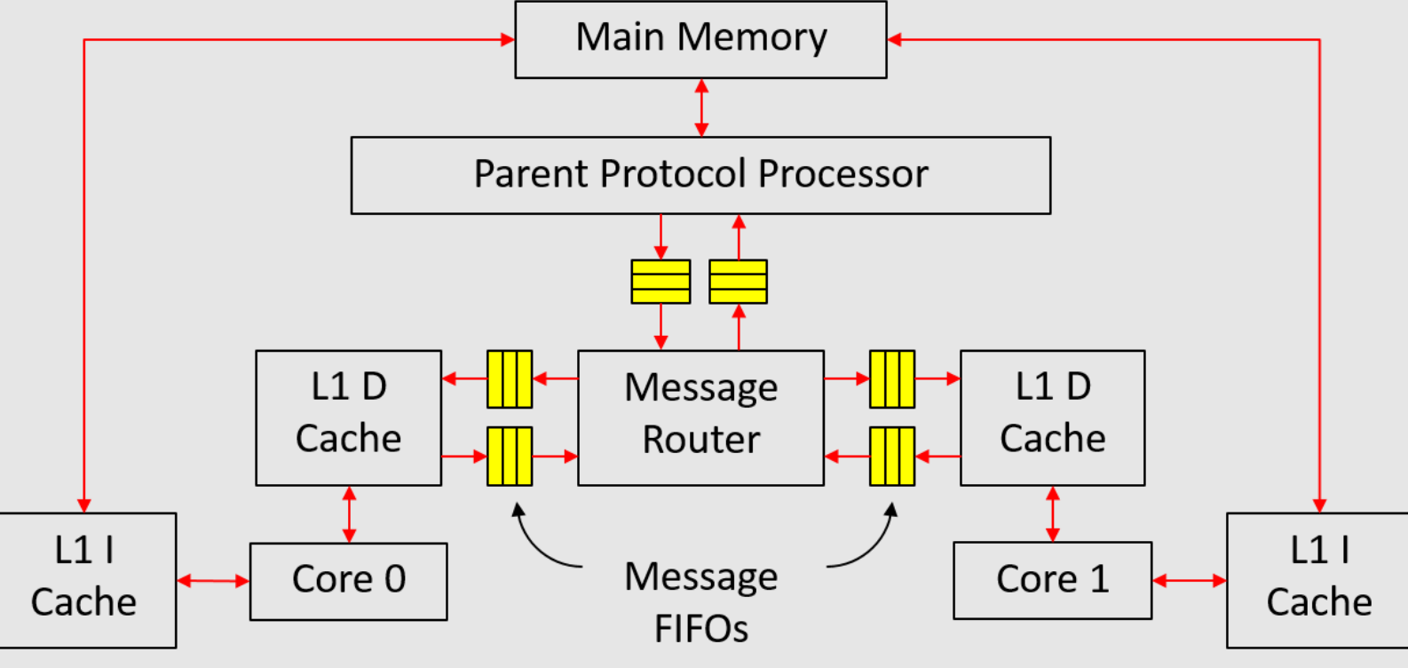 |
|---|
| 图1:多核系统 |
由于该系统相当复杂,我们尝试将实现分为多个小步骤,并为每个步骤提供了测试台。但是,通过测试台并不意味着实现是100%正确的。
实现存储层次结构的单元
消息FIFO
消息FIFO传输请求和响应消息。对于从子级到父级的消息FIFO,它传输升级请求和降级响应。对于从父级到子级的消息FIFO,它传输降级请求和升级响应。
消息FIFO传输的消息类型在src/includes/CacheTypes.bsv中定义如下:
#![allow(unused)]
fn main() {
typedef struct {
  CoreID            child;
  Addr              addr;
  MSI               state;
  Maybe#(CacheLine) data;
} CacheMemResp deriving(Eq, Bits, FShow);

typedef struct {
  CoreID      child;
  Addr        addr;
  MSI         state;
} CacheMemReq deriving(Eq, Bits, FShow);

typedef union tagged {
  CacheMemReq     Req;
  CacheMemResp    Resp;
} CacheMemMessage deriving(Eq, Bits, FShow);
}
CacheMemResp是从子级到父级的降级响应以及从父级到子级的升级响应的类型。第一个字段child是消息传递中涉及的D缓存的ID。CoreID类型在Types.bsv中定义。第三个字段state是子级为降级响应降级到的MSI状态,或子级可以为升级响应升级到的MSI状态。
CacheMemReq是从子级到父级的升级请求和从父级到子级的降级请求的类型。第三个字段state是子级想要为升级请求升级到的MSI状态,或子级应该为降级请求降级到的MSI状态。
消息FIFO的接口也在CacheTypes.bsv中定义:
#![allow(unused)]
fn main() {
interface MessageFifo#(numeric type n);
  method Action enq_resp(CacheMemResp d);
  method Action enq_req(CacheMemReq d);
  method Bool hasResp;
  method Bool hasReq;
  method Bool notEmpty;
  method CacheMemMessage first;
  method Action deq;
endinterface
}
接口有两个入队方法(enq_resp和enq_req),一个用于请求,另一个用于响应。布尔标志hasResp和hasReq分别表示FIFO中是否有任何响应或请求。notEmpty标志只是hasResp和hasReq的或运算。接口只有一个first和一个deq方法,一次检索一条消息。
如课堂上所述,当它们都位于同一个消息FIFO中时,请求永远不应阻止响应。为了确保这一点,我们可以使用两个FIFO实现消息FIFO,如图2所示。在入队端,所有请求都入队到请求FIFO,而所有响应都入队到另一个响应
FIFO。在出队端,响应FIFO优先于请求FIFO,即只要响应FIFO不为空,deq方法就应该出队响应FIFO。接口定义中的数值类型n是响应/请求FIFO的大小。
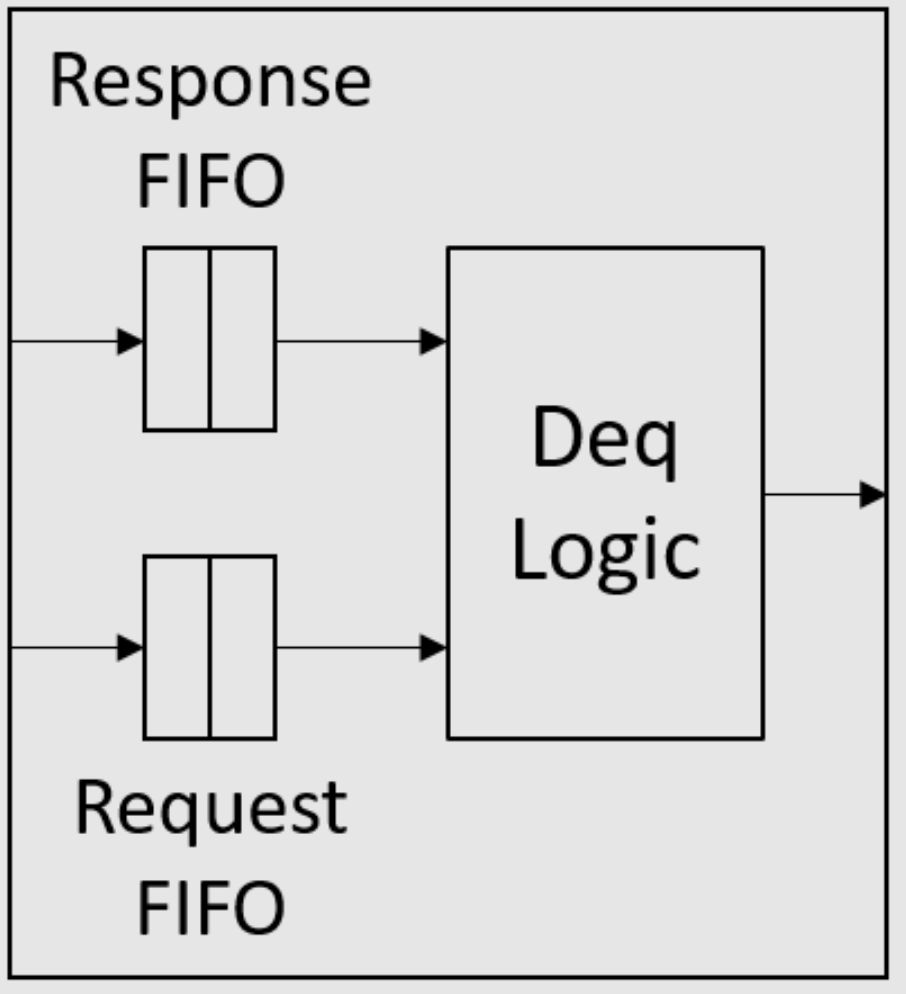 |
|---|
| 图2:消息FIFO的结构 |
**练习1(10分):**在
src/includes/MessageFifo.bsv中实现消息FIFO(mkMessageFifo模块)。我们在unit_test/message-fifo-test文件夹中提供了一个简单的测试。使用make编译,并使用./simTb运行测试。
消息路由器
消息路由器连接所有L1 D缓存和父协议处理器。我们将在src/includes/MessageRouter.bsv中实现这个模块。它声明为:
module mkMessageRouter(
  Vector#(CoreNum, MessageGet) c2r, Vector#(CoreNum, MessagePut) r2c,
  MessageGet m2r, MessagePut r2m,
  Empty ifc
);
MessageGet和MessagePut接口只是MessageFibo接口的限制视图,它们在CacheTypes.bsv中定义:
interface MessageGet;
  method Bool hasResp;
  method Bool hasReq;
  method Bool notEmpty;
  method CacheMemMessage first;
  method Action deq;
endinterface
interface MessagePut;
  method Action enq_resp(CacheMemResp d);
  method Action enq_req(CacheMemReq d);
endinterface
我们提供了toMessageGet和toMessagePut函数,将MessageFifo接口转换为MessageGet和MessagePut接口。以下是每个模块参数的介绍:
c2r是每个L1 D缓存的消息FIFO的接口。r2c是到每个L1 D缓存的消息FIFO的接口。m2r是来自父协议处理器的消息FIFO的接口。r2m是到父协议处理器的消息FIFO的接口。
此模块的主要功能分为两部分:
- 将消息从父级(
m2r)发送到正确的L1 D缓存(r2c), - 将消息从L1 D缓存(
c2r)发送到父级(r2m)。
应该注意的是,响应消息优先于请求消息,就像消息FIFO中的情况一样。
**练习2(10分):**在
src/includes/MessageRouter.bsv中实现mkMessageRouter模块。我们在unit_test/message-router-test文件夹中提供了一个简单的测试。运行以下命令进行编译和运行:$ make $ ./simTb
L1数据缓存
阻塞L1 D缓存(不带存储队列)将在src/includes/DCache.bsv中实现:
module mkDCache#(CoreID id)(MessageGet fromMem, MessagePut toMem, RefDMem refDMem, DCache ifc);
以下是每个模块参数和参数的介绍:
id是核心ID,它将附加到发送到父协议处理器的每条消息上。fromMem是来自父协议处理器的消息FIFO的接口(或更准确地说是消息路由器),因此可以从此接口读出降级请求和升级响应。toMem是到父协议处理器的消息FIFO的接口,因此应将升级请求和降级响应发送到此接口。refDMem用于调试,目前你不需要担心它。
模块返回的`
DCache接口在CacheTypes.bsv`中定义如下:
interface DCache;
  method Action req(MemReq r);
  method ActionValue#(MemResp) resp;
endinterface
你可能已经注意到MemOp类型(在MemTypes.bsv中定义),它是MemReq结构体(在MemTypes.bsv中定义)的op字段的类型,现在有五个值:Ld, St, Lr, Sc和Fence。现在你只需要处理Ld和St请求。你可以在DCache接口的req方法中添加逻辑,如果检测到除Ld或St之外的请求则报告错误。
MemReq类型还有一个新字段rid,这是用于调试的请求ID。rid是Bit\#(32)类型,对于同一核心的每个请求应该是唯一的。
我们将实现一个16条目直接映射的L1 D缓存(缓存行数定义为CacheTypes.bsv中的类型CacheRows)。我们建议使用寄存器向量来实现缓存数组以分配初始值。我们还在CacheTypes.bsv中提供了一些有用的函数。
MSI状态类型在CacheTypes.bsv中定义:
typedef enum {M, S, I} MSI deriving(Bits, Eq, FShow);
我们使MSI类型成为Ord类型类的一个实例,因此我们可以在它上面应用比较运算符(>, <, >=, <=等)。顺序是M > S > I。
**练习3(10分):**在
src/includes/DCache.bsv中实现mkDCache模块。这应该是一个不带存储队列的阻塞缓存。你可能想使用最终项目第一部分练习1中的变通方法,以避免将来在D缓存集成到处理器流水线时的调度冲突。我们在unit_test/cache-test文件夹中提供了一个简单的测试。要编译和测试,请运行$ make $ ./simTb
父协议处理器
父协议处理器将在src/includes/PPP.bsv中实现:
module mkPPP(MessageGet c2m, MessagePut m2c, WideMem mem, Empty ifc);
以下是每个模块参数的介绍:
c2m是来自L1 D缓存的消息FIFO的接口(实际上来自消息路由器),可以从此接口读出升级请求和降级响应。m2c是到L1 D缓存的消息FIFO的接口(实际上到消息路由器),应将降级请求和升级响应发送到此接口。mem是主内存的接口,我们已经在项目的第一部分中使用过。
在讲座中,父协议处理器中的目录记录了每个可能地址的MSI状态。然而,对于32位地址空间,这将占用大量存储空间。为了减少目录所需的存储量,我们注意到我们只需要跟踪存在于L1 D缓存中的地址。具体来说,我们可以按照以下方式实现目录:
Vector#(CoreNum, Vector#(CacheRows, Reg#(MSI))) childState <- replicateM(replicateM(mkReg(I)));
Vector#(CoreNum, Vector#(CacheRows, Reg#(CacheTag))) childTag <- replicateM(replicateM(mkRegU));
当父协议处理器想要了解核心i上地址a的大致MSI状态时,它可以首先读出tag=childTag[i][getIndex(a)]。如果tag与getTag(a)不匹配,则MS
I状态必须是I。否则,状态应该是childState[i][getIndex(a)]。通过这种方式,我们大大减少了目录所需的存储量,但我们需要在子状态发生任何变化时维护childTag数组。
与讲座中的另一个不同之处在于,主内存数据应使用mem接口访问,而讲座只是假设组合读取数据。
**练习4(10分):**在
src/includes/PPP.bsv中实现mkPPP模块。我们在unit_test/ppp-test文件夹中提供了一个简单的测试。使用make编译,并使用./simTb运行测试。
测试整个存储层次结构
既然我们已经构建了存储系统的每个部分,现在我们将它们放在一起,并使用uint_test/sc-test文件夹中的测试台测试整个存储层次结构。测试将利用mkDCache的"RefDMem refDMem"参数,并且我们需要在mkDCache中添加一些对refDMem方法的调用。refDMem由一个用于一致内存的参考模型(在src/ref/RefSCMem.bsv中的mkRefSCMem)返回,该模型可以基于对refDMem方法的调用检测一致性违规。RefDMem在src/ref/RefTypes.bsv中定义如下:
interface RefDMem;
  method Action issue(MemReq req);
  method Action commit(MemReq req, Maybe#(CacheLine) line, Maybe#(MemResp) resp);
endinterface
对于mkDCache中的req方法中的每个请求,都应调用issue方法:
method Action req(MemReq r);
  refDMem.issue(r);
  // 然后处理r
endmethod
这将告诉参考模型发送到D缓存的所有请求的程序顺序。
当请求处理完成时,应调用commit方法,即当Ld请求获得加载结果或St请求写入缓存的数据数组时。以下是commit的每个方法参数的介绍:
-
req是正在提交(即完成处理)的请求。 -
line是req正在访问的缓存行的原始值。这里的缓存行是指具有行地址getLineAddr(req.addr)的64B数据块。因此,它不一定是指D缓存中的行,因为D缓存可能只包含垃圾数据。由于line是原始值,在提交存储请求的情况下,它应该是存储修改之前的值。如果我们知道缓存行数据,
line应设置为tagged Valid。否则,我们将line设置为tagged Invalid。在mkDCache的情况下,当请求提交时,我们总是知道缓存行数据,因为它要么已经在D缓存中,要么在来自父级的升级响应中。因此,line应始终设置为tagged Valid。 -
resp是发送回核心的req的响应。如果有响应发送回核心,则resp应为tagged Valid response;否则应为tagged Invalid。对于Ld请求,resp应为tagged Valid (load result)。对于St请求,resp应为tagged Invalid,因为D缓存从不为St请求发送响应。
当mkDCache调用commit(req, line, resp)方法时,一致内存的参考模型将检查以下事项:
- 是否可以提交
req。如果req尚未发出(即从未为req调用issue方法),或者同一核心的一些较
旧请求尚未提交(即非法重新排序内存请求),则不能提交req。
2. 缓存行值line是否正确。如果line是Invalid,则不执行检查。
3. 响应resp是否正确。
uint_test/sc-test文件夹中的测试台实例化了一个完整的内存系统,并向每个L1 D缓存提供随机请求。它依赖于参考模型来检测内存系统内部的一致性违规。
**练习5(10分):**在
src/includes/DCache.bsv中的mkDCache模块中添加对refDMem方法的调用。然后进入uint_test/sc-test文件夹,使用make编译测试台。这将创建两个仿真二进制文件:simTb_2用于两个D缓存,simTb_4用于四个D缓存。你也可以分别通过make tb_2和make tb_4编译它们。运行测试:
$ ./simTb_2 > dram_2.txt和
$ ./simTb_4 > dram_4.txt
dram_*.txt将包含mkWideMemFromDDR3模块的调试输出,即与主内存的请求和响应。主内存由mem.vmh初始化,这是一个空的VMH文件。这将初始化主内存的每个字节为0xAA。
请求发送到D缓存i的跟踪可以在driver_<i>_trace.out中找到。
测试程序
我们可以使用以下命令编译测试程序:
$ cd programs/assembly
$ make
$ cd ../benchmarks
$ make
$ cd ../mc_bench
$ make
$ make -f Makefile.tso
programs/assembly 和 programs/benchmarks 包含单核心的汇编和基准测试程序。在这些程序中,只有核心0会执行程序,而核心1将在启动后不久进入 while(1) 循环。
programs/mc_bench 包含多核基准测试程序。在这些程序的主函数中,首先获取核心ID(即 mhartid CSR),然后根据核心ID跳转到不同的函数。一些程序只使用普通的加载和存储,而其他程序则使用原子指令(加载保留和条件存储)。
我们已经在 scemi/sim 文件夹中提供了多个脚本来运行测试程序。这些脚本都可以用以下方式调用:
$ ./<script name>.sh <proc name>
将处理器集成到存储层次结构中
在测试存储系统之后,我们开始将其集成到多核系统中。我们已经在 src/Proc.bsv 中提供了多核系统的代码,其中实例化了一致内存的参考模型、主内存、核心、消息路由器和父协议处理器。我们已经讨论了 Proc.bsv 中的所有内容,除了核心(mkCore 模块)。我们将使用两种类型的核心:三周期核心和六阶段流水线核心。Proc.bsv 中的宏 CORE_FILE 控制我们使用哪种类型的核心。
请注意,Proc.bsv 中有两种类型的参考模型,mkRefSCMem 和 mkRefTSOMem,实例化由一些宏控制。mkRefSCMem 是没有任何存储队列的阻塞缓存的内存系统的参考模型,而 mkRefTSOMem 是包含存储队列的缓存的内存系统的参考模型。目前我们将使用 mkRefSCMem,因为我们还没有在我们的缓存中引入存储队列。
三周期核心
我们已经在 src/ThreeCycle.bsv 中提供了三周期核心的实现:
module mkCore#(CoreID id)(WideMem iMem, RefDMem refDMem, Core ifc);
iMem 参数传递给 I 缓存(与项目第一部分的 I 缓存相同)。由于 I 缓存数据本质上是一致的,它可以直接将 refDMem 参数传递给 D 缓存,以便我们可以借助参考模型进行调试。Core 接口在 src/includes/ProcTypes.bsv 中定义。
这段代码中有一点值得注意:我们实例化了一个 mkMemReqIDGen 模块来为发送到 D 缓存的每个请求生成 rid 字段。至关重要的是,同一核心发出的每个 D 缓存请求都有一个 rid,因为一致内存的参考模型依赖于 rid 字段来识别请求。mkMemReqIDGen 模块在 MemReqIDGen.bsv 中实现,这个模块只是一个32位计数器。
尽管代码会向 D 缓存发出除 Ld 或 St 之外的请求,我们在以下练习中运行的程序只会使用普通的加载和存储。
**练习6(10分):**从项目的第一部分复制
ICache.bsv到src/includes/ICache.bsv。转到scemi/sim文件夹,并使用三周期核心编译多核系统 `build -v th
reecache。使用脚本 run_asm.sh、run_bmarks.sh和run_mc_no_atomic.sh测试处理器。脚本run_mc_no_atomic.sh` 运行只使用普通加载和存储的多核程序。
六阶段流水线核心
**练习7(10分):**在
src/SixStage.bsv中实现六阶段流水线核心。代码应该与你在项目的第一部分中实现的非常相似。你还需要从项目的第一部分复制Bht.bsv到src/includes/Bht.bsv。你可能还想参考ThreeCycle.bsv中的一些细节(例如生成请求ID)。
注意:助教建议在流水线中使用无冲突的寄存器文件和计分板,因为 Bluespec 编译器将寄存器读取规则与回写规则安排为冲突,而助教的实现使用的是旁路寄存器文件和流水线计分板。
转到 scemi/sim 文件夹,并使用三周期核心编译多核系统 build -v sixcache。使用脚本 run_asm.sh、run_bmarks.sh 和 run_mc_no_atomic.sh 测试处理器。
原子内存访问指令
在现实生活中,多核程序使用原子内存访问指令来更有效地实现同步。现在我们将在 RISC-V 中实现 load-reserve (lr.w) 和 store-conditional (sc.w) 指令。这两条指令都访问内存中的一个字(如 lw 和 sw),但它们带有特殊的副作用。
我们已经为这两条指令实现了内存系统外部所需的所有内容(参见 ThreeCycle.bsv)。lr.w 的 iType 为 Lr,对应的 D 缓存请求的 op 字段也是 Lr。在回写阶段,lr.w 将加载结果写入目的寄存器。sc.w 的 iType 为 Sc,对应的 D 缓存请求的 op 字段也是 Sc。在回写阶段,sc.w 将从 D 缓存返回的值(表明此条件存储是否成功)写入目的寄存器。
支持这两条指令的唯一剩余事项是改变我们的 D 缓存。请注意,父协议处理器不需要任何更改。
我们需要在 mkDCache 中添加一个新的状态元素:
Reg#(Maybe#(CacheLineAddr)) linkAddr <- mkReg(Invalid);
此寄存器记录由 lr.w 保留的缓存行地址(如果寄存器有效)。以下是 D 缓存中处理 Lr 和 Sc 请求的行为总结:
-
Lr可以像普通的Ld请求一样在 D 缓存中处理。当此请求处理完成时,它将linkAddr设置为tagged Valid (accessed cache line address)。 -
处理
Sc请求时,我们首先检查linkAddr中保留的地址是否与Sc请求访问的地址匹配。如果linkAddr无效或地址不匹配,我们直接以值 1 响应核心,表示条件存储操作失败。否则,我们继续将其作为St请求处理。如果在缓存中命中(即缓存行处于M状态),我们将写入数据数组,并以值 0 响应核心,表示条件存储操作成功。在存储未命中的情况下,当我们从父级获取升级响应时,我们需要再次检查linkAddr。如果匹配,我们执行写入并返回 0 给核心;否则我们只返回 1 给核心。我们在
ProcTypes.bsv中提供了scFail和scSucc常量来表示Sc请求的返回值。当
Sc请求处理完成时,无论成功与否,它总是将linkAddr设置为tagged Invalid。
关于 linkAddr 的另一点是,当相应的缓存行离开 D 缓存时,必须将其设置为 tagged Invalid。也就是说,当一个缓存行被从 D 缓存中驱逐时(例如由于替换或失效请求),必须检查缓存行地址是否与 linkAddr 匹配。如果匹配,则应将 linkAddr 设置为 tagged Invalid。
练习8(20分): 修改
src/includes/DCache.bsv和src/SixStage.bsv以处理lr.w和sc.w指令。注意,在mkDCache中也需要适当地调用refDMem接口的方法来处理Lr和Sc请求。对于refDMem接口的commit方法,最后一个参数resp对于Lr和Sc请求都应为tagged Valid (response to core)。commit方法的第二
个参数 line 在某些情况下可能设置为 tagged Invalid,因为我们并不总是知道请求提交时的缓存行值。
>
>转到 scemi/sim 文件夹,并使用以下命令为三周期和六阶段处理器构建:
>
> >$ build -v threecache >
>
>和
>
> >build -v sixcache >
>
>使用脚本 run_asm.sh, run_bmarks.sh 和 run_mc_all.sh 测试处理器。脚本 run_mc_all.sh 将运行所有多核程序,其中一些使用 lr.w 和 sc.w。
添加存储队列
现在我们将在 D 缓存中添加存储队列,以隐藏存储未命中的延迟,就像我们在项目的第一部分所做的那样。引入存储队列将使我们的处理器的编程模型从顺序一致性(SC)变为总存储顺序(TSO),这就是为什么我们将参考模型命名为 mkRefSCMem 和 mkRefTSOMem 的原因。在接下来的练习中,宏定义将自动选择 mkRefTSOMem 作为参考模型。
由于编程模型不再是 SC,我们需要在 RISC-V 中实现 fence 指令来排序内存访问,但你需要在 D 缓存中添加对它的支持。我们已经实现了内存系统外部 fence 指令所需的一切(见 ThreeCycle.bsv)。fence 指令的 iType 是 Fence,对应的 D 缓存请求的 op 字段也是 Fence。
除了新的 fence 指令外,D 缓存中 Lr 和 Sc 请求的行为也需要澄清。以下是带有存储队列的 D 缓存中所有请求的行为总结:
Ld请求即使在存储队列不为空时也可以处理,并且可以从存储队列绕过数据。St请求总是进入存储队列。Lr或Sc请求只有在存储队列为空时才能开始处理。然而,在处理Lr或Sc请求期间,存储队列可能变得不为空。Fence请求只有在存储队列为空且没有其他请求正在处理时才能处理。处理Fence请求只是简单地移除此请求,不向核心发送任何响应。
请注意我们的 D 缓存总是按顺序处理请求,因此如果一个请求不能被处理,所有后续请求将被阻塞。
将存储从存储队列移动到缓存的过程几乎与项目的第一部分相同。也就是说,这种移动操作只有在有 Ld 请求进入或有其他请求正在处理时才会停止。
练习9(15分): 在
src/includes/DCacheStQ.bsv中实现带存储队列的阻塞 D 缓存(不包含 在存储未命中下加载命中)模块,并修改SixStage.bsv以支持fence指令。注意,在mkDCache中也需要适当地调用refDMem接口的方法来处理Fence请求。对于refDMem接口的commit方法,line和resp参数对于Fence请求应都设置为tagged Invalid。转到
scemi/sim文件夹,并使用build -v threestq和build -v sixstq构建三周期和六阶段处理器。使用脚本run_asm.sh、run_bmarks.sh和run_mc_tso.sh测试处理器。脚本run_mc_tso.sh将运行所有带围栏的多核程序,以符合 TSO 编程模型。实际上,只有mc_dekker程序需要添加围栏。
在引入存储队列后,你应该会看到汇编测试 stq.S 的性能提升。可能的 IPC 数字与项目的第一部分不同,因为在这部分中主内存有轻微的变化。
在存储未命中下加载命中
现在我们将在项目的第一部分中完成的优化应用于
我们的 D 缓存,即允许在存储未命中下加载命中。具体来说,如果 St 请求正在等待来自父级的响应,并且在这个周期内没有来自父级的消息,那么一个命中缓存或存储队列的传入 Ld 请求可以被处理。
练习10(5分): 在
src/includes/DCacheLHUSM.bsv中实现在存储未命中下加载命中的 D 缓存。转到scemi/sim文件夹,并使用build -v threelhusm和build -v sixlhusm构建三周期和六阶段处理器。使用脚本run_asm.sh、run_bmarks.sh和run_mc_tso.sh测试处理器。
在引入存储队列后,你应该会看到单核基准测试 tower 的性能提升。可能的 IPC 数字与项目的第一部分不同,因为在这部分中主内存有轻微的变化。
为处理器添加更多功能(额外奖励)
现在你已经拥有了一个成熟的多核系统,如果你有时间,可以开始探索新事物。以下是一些你可以尝试的示例方向:
- 新的多核程序,例如一些并发算法。
- 更好的调试基础设施。
- 优化存储队列:使其无序。
- 非阻塞缓存和父协议处理器。
- 实现虚拟内存和 TLBs。
- 为 FPGA 合成你的多核系统。
- 使用 RoCC 接口的应用特定加速器/协处理器。
- 采用 MIPS R10000 或 Alpha 21264 风格的乱序超标量处理器。(如果你这样做,我们想和你聊聊。)
最终展示
别忘了通过提交更改并将它们推回你的学生仓库来提交你的代码。
12月14日下午3点至6点,我们将举行这个项目的最终展示,并在最后提供一些比萨饼。我们希望你准备一个不超过10分钟的关于你的最终项目的展示。你应该谈论以下几点:
- 组内成员如何分工。
- 你遇到了哪些困难或错误,以及你是如何解决它们的。
- 你添加的(或你仍在添加的)新东西。
© 2016 麻省理工学院。版权所有。
MIT-6.175 Introduction/Contents
What is 6.175?
6.175 teaches the fundamental principles of computer architecture via implementation of different versions of pipelined machines with caches, branch predictors and virtual memory. Emphasis on writing and evaluating architectural descriptions that can be both simulated and synthesized into real hardware or run on FPGAs. The use and design of test benches. Weekly labs. Intended for students who want to apply computer science techniques to complex hardware design.
Topics include combinational circuits including adders and multipliers, multi-cycle and pipelined functional units, RISC Instruction Set Architectures (ISA), non-pipelined and multi-cycle processor architectures, 2- to 10-stage in-order pipelined architectures, processors with caches and hierarchical memory systems, TLBs and page faults, I/O interrupts.
Instructors
- Arvind
- Quan Nguyen (TA)
Lectures
MWF 3:00 pm, 34-302.
Lab Assignments Directory
- MIT-6.175 Introduction/Contents
- Lab 0: Getting Started
- Lab 1: Multiplexers and Adders
- Lab 2: Multipliers
- Lab 3: FFT Pipeline
- Lab 4: N-Element FIFOs
- Lab 5: RISC-V Introduction - Multi-cycle and Two-Stage Pipelines
- Lab 6: RISC-V Processor with 6-Stage Pipeline and Branch Prediction
- Lab 7: RISC-V Processor with DRAM and Caches
- Lab 8: RISC-V Processor with Exceptions
Project
Schedule
Please check back frequently as this schedule may change.
This calendar is also available on Google Calendar.
| Week | Date | Description | Downloads |
|---|---|---|---|
| 1 | Wed, Sept 7 | Lecture 1: Introduction | [pptx] [pdf] |
| Fri, Sept 9 | Lecture 2: Combinational Circuits Lab 0 out, Lab 1 out | [pptx] [pdf] | |
| 2 | Mon, Sept 12 | Lecture 3: Combinational Circuits 2 | [pptx] [pdf] |
| Wed, Sept 14 | Lecture 4: Sequential Circuits | [pptx] [pdf] | |
| Fri, Sept 16 | Lecture 5: Sequential Circuits 2 Lab 1 due, Lab 2 out | [pptx] [pdf] | |
| 3 | Mon, Sept 19 | Lecture 6: Pipelining Combinational Circuits | [pptx] [pdf] |
| Wed, Sept 21 | Lecture 7: Well-Formed BSV Programs Ephemeral History Registers | [pptx] [pdf] | |
| Fri, Sept 23 | No classes: Student Holiday (Fall Career Fair) Lab 3 out | ||
| 4 | Mon, Sept 26 | Lecture 8: Multirule Systems and Concurrent Execution of Rules Lab 2 due | [pptx] [pdf] |
| Wed, Sept 28 | Lecture 9: Guards | [pptx] [pdf] | |
| Fri, Sept 30 | Tutorial 1: Bluespec | [pptx] [pdf] | |
| 5 | Mon, Oct 3 | Lecture 10: Non-pipelined Processors Lab 4 out | [pptx] [pdf] |
| Wed, Oct 5 | Lecture 11: Non-pipelined and Pipelined Processors Lab 3 due | [pptx] [pdf] | |
| Fri, Oct 7 | Tutorial 2: Advanced Bluespec | [pptx] [pdf] | |
| 6 | Mon, Oct 10 | No classes: Indigenous Peoples' Day / Columbus Day | |
| Tue, Oct 11 | Lab 5 out | ||
| Wed, Oct 12 | Lecture 12: Control Hazards Lab 4 due | [pptx] [pdf] | |
| Fri, Oct 14 | Tutorial 3: RISC-V Processor RISC-V and Debugging | [pptx] [pdf] | |
| 7 | Mon, Oct 17 | Lecture 13: Data Hazards | [pptx] [pdf] |
| Wed, Oct 19 | Lecture 14: Multistage Pipelines Lab 6 out | [pptx] [pdf] | |
| Fri, Oct 21 | Tutorial 4: Debug Epochs and Scoreboards Lab 5 due | [pptx] [pdf] | |
| 8 | Mon, Oct 24 | Lecture 15: Branch Prediction Lab 5 due | [pptx] [pdf] |
| Wed, Oct 26 | Lecture 16: Branch Prediction 2 | [pptx] [pdf] | |
| Fri, Oct 28 | Tutorial 5: Epochs and Branch Predictors Epochs, Debugging, and Caches | [pptx] [pdf] | |
| 9 | Mon, Oct 31 | Lecture 17: Caches | [pptx] [pdf] |
| Wed, Nov 2 | Lecture 18: Caches 2 Lab 7 out | [pptx] [pdf] | |
| Fri, Nov 4 | Tutorial 6: Caches and Exceptions Lab 6 due | [pptx] [pdf] | |
| 10 | Mon, Nov 7 | Lecture 19: Exceptions Lab 6 due | [pptx] [pdf] |
| Wed, Nov 9 | Lecture 20: Virtual Memory | [pptx] [pdf] | |
| Fri, Nov 11 | No classes: Veterans Day | ||
| 11 | Mon, Nov 14 | Lecture 21: Virtual Memory and Exceptions Lab 8 out | [pptx] [pdf] |
| Wed, Nov 16 | Lecture 22: Cache Coherence Lab 7 due | [pptx] [pdf] | |
| Thu, Nov 17 | Lab 8 out | ||
| Fri, Nov 18 | Tutorial 7: Project Overview Lab 7 due, Project Part 1 out | [pptx] [pdf] | |
| 12 | Mon, Nov 21 | Lecture 23: Sequential Consistency | [pptx] [pdf] |
| Wed, Nov 23 | Tutorial 8: Project Part 2: Coherence Cancelled: (early) Thanksgiving Lab 8 due | ||
| Fri, Nov 25 | No classes: Thanksgiving Lab 8 due | ||
| 13 | Mon, Nov 28 | No classes: Work on project Project Part 2 out | |
| Wed, Nov 30 | No classes: Work on project | ||
| Thu, Dec 1 | Project Part 2 out | ||
| Fri, Dec 2 | No classes: Work on project Tutorial 8: Project Part 2: Coherence | [pptx] [pdf] | |
| 14 | Mon, Dec 5 | No classes: Work on project | |
| Wed, Dec 7 | No classes: Work on project | ||
| Fri, Dec 9 | No classes: Work on project | ||
| 15 | Mon, Dec 12 | No classes: Work on project | |
| Wed, Dec 14 | Last day of classes Project presentations |
© 2016 Massachusetts Institute of Technology. All rights reserved.
Lab 0: Getting Started
Throughout this course, you will use shared machines for working on the labs. These machines include vlsifarm-03.mit.edu through vlsifarm-08.mit.edu. You can log into these machines through ssh using your Athena username and password.
This document will instruct you how do some things required for lab such as obtaining initial code for each lab. Begin by using an ssh client to log into one of the servers named above.
Setting up the toolchain
Execute the following commands to set up your environment and gain access to the tool-chain:
$ add 6.175
$ source /mit/6.175/setup.sh
The first command gives you access to the course locker /mit/6.175 and only needs to be run once per computer. The second command configures your current environment to include tools required for the lab and needs to be run every time you log in to work on classwork.
Using Git to get and submit lab code
The reference designs are provided in Git repositories. You can clone them into your work directory using the following command (substitute labN with the lab number, such as lab1 and lab2):
$ git clone $GITROOT/labN.git
Note: If "git clone" fails, it's probably because we don't have your Athena user name. Send me an email (to qmn mit) and I'll create a remote repository for you.
This command creates a labN directory in your current directory. The $GITROOT environment variable is unique to you, so this repository will be your personal repository. Inside that directory, the test benches can be run using the directions specified in the lab handouts.
Discussion questions should be answered in discussion.txt file supplied with the rest of the code.
If you want to add any new files in addition to what has been supplied by the TAs, you need to add the new file (in this example, newFile in git using:
$ git add newFile
You can locally commit your code whenever you hit a milestone using:
$ git commit -am "Hit milestone"
Submit your code by adding any necessary files and then using:
$ git commit -am "Finished lab"
$ git push
You can submit multiple times before the deadline if necessary.
Writing Bluespec SystemVerilog (BSV) for the labs
On vlsifarm-0x
6.175 will be a great opportunity to learn how to work in a Linux command-line environment if you are not already familiar with it. To test your BSV code, you need to use a Linux environment to run bsc, the BSV compiler. It makes sense to go ahead and write the BSV code on the same machine.
While there are many text editors you can use, there is only Bluespec-provided BSV syntax highlighting for Vim and Emacs. The Vim syntax highlighting files can be installed by running:
$ /mit/6.175/vim_copy_BSV_syntax.sh
The Emacs syntax highlighting files can be found on the course resources page. Your TA used to use Emacs, but converted to Vim. He cannot claim to know how to install the highlighting mode files, or even if they work. If you are an Emacs user and would like to contribute documentation on this matter, please send an email to the course staff.
On the Athena cluster
Your home directory on the vlsifarm machines is the same as your home directory on any Athena machine. Therefore you can write code on an Athena machine using gedit or another graphical text editor and log into a vlsifarm machine to run it.
On your own machine
You can also use file transfer programs to move files between your Athena home directory and your own machine. MIT has help for securely transferring files between machines on the web at http://ist.mit.edu/software/filetransfer.
Compiling BSV on other machines
BSV can also be compiled on non-vlsifarm machines. This may be useful when the vlsifarm machines are busy near lab deadlines.
On the Athena cluster
The instructions used for the vlsifarm machines will also work for the Linux-based Athena machines. Just open a terminal and run the commands as you would run them on the vlsifarm machines.
On your own Linux-based machine
To run the 6.175 labs on your own Linux-based machine, you will need the following software installed on your computer:
- OpenAFS to access the course locker
- Git to access and submit the labs
- GMP (libgmp.so.3) to run the BSV compiler
- Python to run build scripts
Side note: A similar setup may work for Mac OS X / macOS. If you get such a setup working, please provide details to the TA.
OpenAFS
Installing OpenAFS on your local machine will give you access to the directory /afs/athena.mit.edu that contains all of the course lockers. You will have to create your own /mit folder with symlinks within to point to the necessary course lockers.
CSAIL TIG has some information about how to install OpenAFS for Ubuntu at http://tig.csail.mit.edu/wiki/TIG/OpenAFSOnUbuntuLinux. These instructions are for accessing /afs/csail.mit.edu, but you need access to /afs/athena.mit.edu for the lab, so replace csail with athena wherever you see it. When you install OpenAFS on your machine, it gives you a /afs folder with many domains within. This website also contains the instructions for logging in with your user name and password to gain access to the files that require authentication. You will need to do this every day you work on the lab, or every time you reset your computer, in order to access the 6.175 course locker.
Next you need to make a folder named mit in your root directory and populate it with a symlink to the course repository. On Ubuntu and similar distributions, the commands are:
$ cd /
$ sudo mkdir mit
$ cd mit
$ sudo ln -s /afs/athena.mit.edu/course/6/6.175 6.175
You can now access the course locker in the folder /mit/6.175.
Git
On Ubuntu and similar distributions, you can install Git with
$ sudo apt-get install git
GMP (libgmp.so.3)
The BSV Compiler uses libgmp for unbounded integers. To install it on Ubuntu and similar distributions, use the command
$ sudo apt-get install libgmp3-dev
If you have libgmp installed on your machine, but you do not have libgmp.so.3, you can create a symlink named libgmp.so.3 that points to a different version.
Python
On Ubuntu and similar distributions, you can install Python with
$ sudo apt-get install python
Setting up the toolchain on your Linux-based machine
The original setup.sh script will not work on your machine, so instead you will have to use
$ source /mit/6.175/local_setup.sh
to set up the toolchain. Once you have done this, you should be able to use the tools as usual on your own machine.
© 2016 Massachusetts Institute of Technology. All rights reserved.
Lab 1: Multiplexers and Adders
Lab 1 due date: Friday, September 16, 2016, at 11:59:59 PM EDT.
Your deliverables for Lab 1 are:
- your answers to Exercises 1-5, in
Multiplexer.bsvandAdders.bsv, and- your answers to the discussion questions in
discussion.txt.
Introduction
In this lab, you will build multiplexers and adders from basic gate primitives. First, you will build a 1-bit multiplexer using and, or, and not gates. Next, you will write a polymorphic multiplexer using for-loops. Then, you will switch to working with adders, constructing a 4-bit adder using full adders. Lastly, you will modify an 8-bit ripple-carry adder to change it to a carry-select adder.
This lab is used as an introduction to simple combinational circuits and Bluespec SystemVerilog (BSV). Even though BSV contains higher-level functions to create circuits, this lab will focus on using low-level gates to create blocks used in higher-level circuits, such as adders. This stresses the hardware generated by the BSV compiler.
Multiplexers
Multiplexers (or muxes for short) are blocks that select between multiple signals. A multiplexer has multiple data inputs inN, a select input sel, and a single output out. The value of sel determines which input is shown on the output. The muxes in this lab are all 2-way muxes. That means there will be two inputs to select between (in0 and in1) and sel will be a single bit. If sel is 0, then out = in0. If sel is 1, then out = in1. Figure 1a shows the symbol used for a mux, and figure 1b shows pictorially the function of a mux.
 |  |
|---|---|
| (a) Multiplexer symbol | (b) Multiplexer functionality |
Figure 1: Symbol and functionality of 1-bit multiplexer
Adders
Adders are essential building blocks for digital systems. There are many different adder architectures that all compute the same result, but they get to the results in different ways. Different adder architectures also differ in area, speed, and power, and there is no architecture that dominates all other adders in all the areas. Therefore, hardware designers choose adders based on system area, speed, and power constraints.
The adder architectures we are going to explore are the ripple-carry adder and the carry-select adder. The ripple-carry adder is the simplest adder architecture. It is made up of a chain of full adder blocks connected through the carry chain. A 4-bit ripple-carry adder can be seen in figure 2b. It is very small, but it is also very slow because each full adder has to wait for the previous full adder to finish before it can compute its bit.
The carry-select adder adds prediction or speculation to the ripple-carry adder to speed up execution. It computes the bottom bits the same way the ripple-carry adder computes them, but it differs in the way it computes the top bits. Instead of waiting for the carry signal from the lower bits to be computed, it computes two possible results for the top bits: one results assumes there is no carry from the lower bits and the other assumes there is a bit carried over. Once that carry bit is calculated, a mux selects the top bits that correspond to the carry bit. An 8-bit carry-select adder can be seen in figure 3.
 | 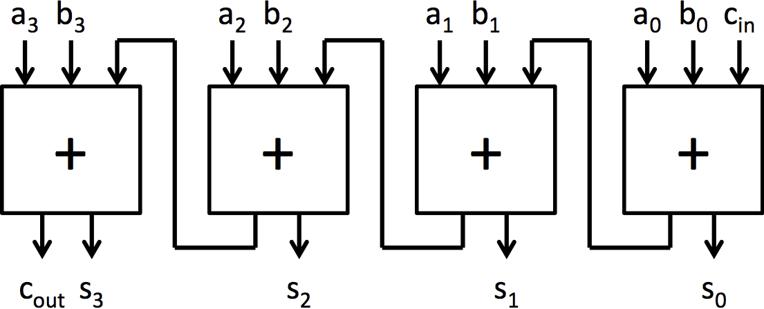 |
|---|---|
| (a) Full adder | (b) 4-bit ripple-carry adder built from full adders |
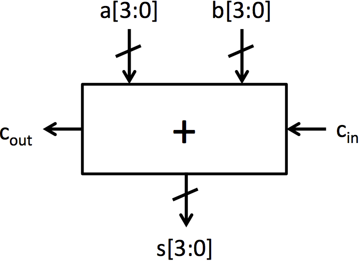 | 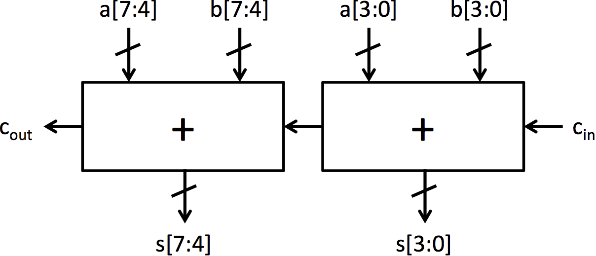 |
|---|---|
| (c) Symbol for 4-bit adder | (d) 8-bit ripple-carry adder |
Figure 2: Construction of a 4-bit adder and an 8-bit adder from full adder blocks
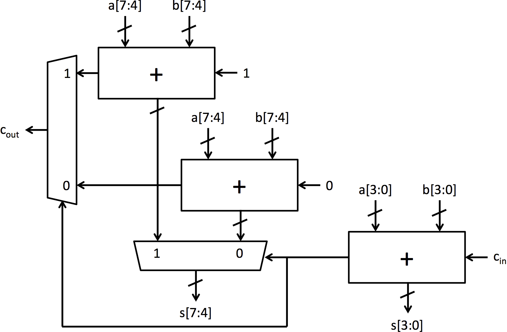 |
|---|
Figure 3: 8-bit carry-select adder
Testbenches
The testbenches to test your code have already been written, and links to the testbenches are included in the repository for this lab. The file TestBench.bsv contains multiple testbenches that can be individually compiled by using the provided Makefile. The Makefile has a target for each simulator executable, and the use of each target and executable is explained in this handout. Each executable prints out PASSED when the program works, and FAILED when the program encounters an error.
The testbenches ending in Simple have a simplified structure, and they output all the data that came from the unit during the test so you can see the unit working. If you are interested in testing your own cases for these units, you can modify the simple testbenches to input the values you request. The normal testbench generates random numbers for input values.
Building multiplexers in BSV
The first step in constructing our carry-select adder is to build a basic multiplexer from gates. Let’s first examine Multiplexer.bsv.
#![allow(unused)]
fn main() {
function Bit#(1) multiplexer1(Bit#(1) sel, Bit#(1) a, Bit#(1) b);
    return (sel == 0)? a: b;
endfunction
}
The first line begins a definition of a new function called multiplexer1. This multiplexer function takes several arguments which will be used in defining the behavior of the multiplexer. This multiplexer operates on single bit values, the concrete type Bit#(1). Later we will learn how to implement polymorphic functions, which can handle arguments of any width.
This function uses C-like constructs in its definition. Simple code, such as the multiplexer can be defined at the high level without implementation penalty. However, because hardware compilation is a dificult, multi-dimensional problem, tools are limited in the kinds of optimizations that they can do.
The return statement, which constitutes the entire function, takes two input and selects between them using sel. The endfunction keyword completes the definition of our multiplexer function. You should be able to compile the module.
Exercise 1 (4 Points): Using the and, or, and not gates, re-implement the function
multiplexer1inMultiplexer.bsv. How many gates are needed? (The required functions, calledand1,or1andnot1, respectively, are provided inMultiplexers.bsv.)
Static elaboration
Many muxes in real world systems are larger than 1-bit wide. We will need multiplexers that are larger than a single bit, but writing the code to manually instantiate 32 single-bit multiplexers to form a 32-bit multiplexer would be tedious. Fortunately, BSV provides constructs for powerful static elaboration which we can use to make writing the code easier. Static elaboration refers to the process by which the BSV compiler evaluates expressions at compile time, using the results to generate the hardware. Static elaboration can be used to express extremely flexible designs in only a few lines of code.
In BSV we can use bracket notation ([]) to index individual bits in a wider Bit type, for example bitVector[1] selects the second least significant bit in bitVector (bitVector[0] selects the least significant bit since BSV's indexing starts at 0). We can use a for-loop to copy many lines of code which have the same form. For example, to aggregate the and1 function to form a 5-bit and function, we could write:
function Bit#(5) and5(Bit#(5) a, Bit#(5) b); Bit#(5) aggregate;
    for(Integer i = 0; i < 5; i = i + 1) begin
        aggregate[i] = and1(a[i], b[i]);
    end
    return aggregate;
endfunction
The BSV compiler, during its static elaboration phase, will replace this for loop with its fully unrolled version.
aggregate[0] = and1(a[0], b[0]);
aggregate[1] = and1(a[1], b[1]);
aggregate[2] = and1(a[2], b[2]);
aggregate[3] = and1(a[3], b[3]);
aggregate[4] = and1(a[4], b[4]);
Exercise 2 (1 Point): Complete the implementation of the function >
multiplexer5inMultiplexer.bsvusing for loops andmultiplexer1. Check the correctness of the code by running the multiplexer testbench:$ make mux $ ./simMuxAn alternate test bench can be used to see outputs from the unit by running:
$ make muxsimple
$ ./simMuxSimple
Polymorphism and higher-order constructors
So far, we have implemented two versions of the multiplexer function, but it is easy to imagine needing an n-bit multiplexer. It would be nice if we did not have to completely re-implement the multiplexer whenever we want to use a different width. Using the for-loops introduced in the previous section, our multiplexer code is already somewhat parametric because we use a constant size and the same type throughout. We can do better by giving a name (N) to the size of the multiplexer using typedef. Our new multiplexer code looks something like:
#![allow(unused)]
fn main() {
typedef 5 N;
function Bit#(N) multiplexerN(Bit#(1) sel, Bit#(N) a, Bit#(N) b);
    // ...
    // code from multiplexer5 with 5 replaced with N (or valueOf(N))
    // ...
endfunction
}
The typedef gives us the ability to change the size of our multiplexer at will. The valueOf function introduces a small subtlety in our code: N is not an Integer but a numeric type and must be converted to an Integer before being used in an expression. Even though it is improved, our implementation is still missing some flexibility. All instantiations of the multiplexer must have the same type, and we still have to produce new code each time we want a new multiplexer. However in BSV we can further parameterize the module to allow different instantiations to have instantiation-specific parameters. This sort of module is polymorphic, the implementation of the hardware changes automatically based on compile time configuration. Polymorphism is the essence of design-space exploration in BSV.
The truly polymorphic multiplexer can be started as follows:
// typedef 32 N; // Not needed
function Bit#(n) multiplexer n(Bit#(1) sel, Bit#(n) a, Bit#(n) b);
The variable n represents the width of the multiplexer, replacing the concrete value N (=32). In BSV type variables (n) start with a lower case whereas concrete types (N) start with an upper case.
Exercise 3 (2 Points): Complete the definition of the function
multiplexer_n. Verify that this function is correct by replacing the original definition ofmultiplexer5to only have:return multiplexer_n(sel, a, b);. This redefinition allows the test benches to test your new implementation without modification.
Building adders in BSV
We will now move on to building adders. The fundamental cell for adding is the full adder which is shown in Figure 2a. This cell adds two input bits and a carry in bit, and it produces a sum bit and a carry out bit. Adders.bsv contains two function definitions that describe the behavior of the full adder. fa_add computes the add output of a full adder, and fa_carry computes the carry output. These functions contain the same logic as the full adder presented in lecture 2.
An adder that operates on 4-bit numbers can be made by chaining together 4 full adders as shown in Figure 2b. This adder architecture is known as a ripple-carry adder because of the structure of the carry chain. To generate this adder without writing out each of the explicit full adders, a for loop can be used similar to multiplexer5.
Exercise 4 (2 Points): Complete the code for
add4by using a for loop to properly connect all the uses offa_sumandfa_carry.
Larger adders can be constructed by connecting 4-bit adders, just like the 4-bit adder was constructed by connecting full adders. Adders.bsv contains two modules for adders constructed using add4 and connecting circuitry: mkRCAdder and mkCSAdder. Note that, unlike the other adders to this point, these adders are implemented as a module instead of a function. This is a subtle, but important distinction. In BSV, functions are inlined by the compiler automatically, while modules must be explicitly instantiated using the '<-' notation. If we made the 8-bit adder a function, using it in multiple locations in BSV code would instantiate multiple adders. By making it a module, multiple sources can use the same 8-bit adder.
The full implementation for the 8-bit ripple-carry adder shown in Figure 2d is included in the module mkRCAdder. It can be tested by running the following:
$ make rca
$ ./simRca
Since mkRCAdder is constructed by combining add4 instances, running ./simRCA will also test add4. An alternate test bench can be used to see outputs from the unit by running:
$ make rcasimple
$ ./simRcaSimple
There is also a mkCSAdder module that is intended to implement the carry-select adder shown in Figure 3, but its implementation is not included.
Exercise 5 (5 Points): Complete the code for the carry-select adder in the module
mkCSAdder. Use Figure 3 as a guide for the required hardware and connections. This module can be tested by running the following:$ make csa $ ./simCsaAn alternate test bench can be used to see outputs from the unit by running:
$ make csasimple
$ ./simCsaSimple
Discussion Questions
Write your answers to these questions in the text file
discussion.txtprovided with the initial lab code.
- How many gates does your one-bit multiplexer use? The 5-bit multiplexer? Write down a formula for the number of gates in an N-bit multiplexer. (2 Points)
- Assume a single full adder requires 5 gates. How many gates does the 8-bit ripple-carry adder require? How many gates does the 8-bit carry-select adder require? (2 Points)
- Assume a single full adder requires A time unit to compute its outputs once all its inputs are valid and a mux requires M time unit to compute its output. In terms of A and M, how long does the 8-bit ripple-carry adder take? How long does the 8-bit carry-select adder take? (2 Points)
- Optional: How long did you take to work on this lab?
When you're done, add any necessary files to the repository using git add, commit the changes with git commit -am "Final submission", and push the modifications for grading with git push.
© 2016 Massachusetts Institute of Technology. All rights reserved.
Lab 2: Multipliers
Lab 2 due date: Monday, September 26, 2016, at 11:59:59 PM EDT. Your deliverables for Lab 2 are:
- your answers to Exercises 1-9, in
Multipliers.bsvandTestBench.bsv, and- your answers to Discussion Questions 1-5 in
discussion.txt.
Introduction
In this lab you will be building different multiplier implementations and testing them using custom instantiations of provided test bench templates. First, you will implement multipliers using repeated addition. Next, you will implement a Booth Multiplier using a folded architecture. Finally, you will build a faster multiplier by implementing a radix-4 Booth Multiplier.
The output of all of these modules will be tested with test benches that compare the output of the modules to BSV's * operator for functionality.
All of the materials for this lab are in the git repository $GITROOT/lab2.git. All discussion questions asked throughout this lab should be answered in discussion.txt. When you have completed the lab, commit your changes to the repository and push the changes.
Built-in Multiplication
BSV has a built-in operation for multiplication: *. It is either a signed or unsigned multiply depending on the types of the operands. For Bit#(n) and UInt#(n), the * operator performs unsigned multiplication. For Int#(n), it performs signed multiplication. Just like the + operator, the * operator assumes the inputs and the output are all the same type. If you want a 2n-bit result from n-bit operands, you have to first extend the operands to be 2n-bit values.
Multipliers.bsv contains functions for signed and unsigned multiplication on Bit#(n) inputs. Both functions return Bit#(TAdd#(n,n)) outputs. The code for these functions are shown below:
Note:
packandunpackare built-in functions that convert to and fromBit#(n)respectively.
#![allow(unused)]
fn main() {
function Bit#(TAdd#(n,n)) multiply_unsigned( Bit#(n) a, Bit#(n) b );
    UInt#(n) a_uint = unpack(a);
    UInt#(n) b_uint = unpack(b);
    UInt#(TAdd#(n,n)) product_uint = zeroExtend(a_uint) * zeroExtend(b_uint);
    return pack( product_uint );
endfunction

function Bit#(TAdd#(n,n)) multiply_signed( Bit#(n) a, Bit#(n) b );
    Int#(n) a_int = unpack(a);
    Int#(n) b_int = unpack(b);
    Int#(TAdd#(n,n)) product_int = signExtend(a_int) * signExtend(b_int);
    return pack( product_int );
endfunction
}
These functions will be the benchmark functions that your multipliers in this lab will be compared to for functionality.
Test Benches
This lab has two parameterized test bench templates that can be easily instantiated with specific parameters to test two multiplication functions against each other, or to test a multiplier module against a multiplier function. These parameters include functions and module interfaces. mkTbMulFunction compares the output of two functions with the same random inputs, and mkTbMulModule compares the outputs of a test module (the device under test or DUT) and a reference function with the same random inputs.
The following code shows how to implement test benches for specific functions and/or modules.
#![allow(unused)]
fn main() {
(* synthesize *)
module mkTbDumb();
    function Bit#(16) test_function( Bit#(8) a, Bit#(8) b ) = multiply_unsigned( a, b );
    Empty tb <- mkTbMulFunction(test_function, multiply_unsigned, True);
    return tb;
endmodule

(* synthesize *)
module mkTbFoldedMultiplier();
    Multiplier#(8) dut <- mkFoldedMultiplier();
    Empty tb <- mkTbMulModule(dut, multiply_signed, True);
    return tb;
endmodule
}
The two lines below instantiate a specific test bench using the test bench templates in TestBenchTemplates.bsv.
Empty tb <- mkTbMulFunction(test_function, multiply_unsigned, True);
Empty tb <- mkTbMulModule(dut, multiply_signed, True);
The first parameter in each (test_function and dut) is the function or the module to test. The second parameter (multiply_unsigned and multiply_signed) is the correctly implemented reference function. In this case, the reference functions were created using BSV's * operator. The last parameter is a boolean that designates if you want a verbose output. If you just want PASSED or FAILED to be printed by the test bench, set the last parameter to False.
These test benches (mkTbDumb and mkTbFoldedMultiplier) can be easily built using the provided Makefile. To compile these examples, you would write make Dumb.tb for the first and make FoldedMultiplier.tb for the second. The makefile will produce the executables simDumb and simFoldedMultiplier. To compile your own test bench mkTb<name>, run
$ make <name>.tb
$ ./sim<name>
There are no .tb files produced by the compilation process, the extension is just used to signal what build target should be used.
Exercise 1 (2 Points): In
TestBench.bsv, write a test benchmkTbSignedVsUnsignedthat tests ifmultiply_signedproduces the same output asmultiply_unsigned. Compile this test bench as described above and run it. (That is, run$ make SignedVsUnsigned.tband then
$ ./simSignedVsUnsigned)
Discussion Question 1 (1 Point): Hardware-wise, unsigned addition is the same as signed addition when using two's complement encoding. Using evidence from the test bench, is unsigned multiplication the same as signed multiplication?
Discussion Question 2 (2 Points): In
mkTBDumbexcluding the line#![allow(unused)] fn main() { function Bit#(16) test_function( Bit#(8) a, Bit#(8) b ) = multiply_unsigned( a, b ); }and modifying the rest of the module to have
#![allow(unused)]
fn main() {
(* synthesize *)
module mkTbDumb();
    Empty tb <- mkTbMulFunction(multiply_unsigned, multiply_unsigned, True);
    return tb;
endmodule
}
will result in a compilation error. What is that error? How does the original code fix the compilation error? You could also fix the error by having two function definitions as shown below.
#![allow(unused)]
fn main() {
(* synthesize *)
module mkTbDumb();
    function Bit#(16) test_function( Bit#(8) a, Bit#(8) b ) = multiply_unsigned( a, b );
    function Bit#(16) ref_function( Bit#(8) a, Bit#(8) b ) = multiply_unsigned( a, b );
    Empty tb <- mkTbMulFunction(test_function, ref_function, True);
    return tb;
endmodule
}
Why is two function definitions not necessary? (i.e. why can the second operand to
mkTbMulFunctionhave variables in its type?) Hint: Look at the types of the operands ofmkTbMulFunctioninTestBenchTemplates.bsv.
Implementing Multiplication by Repeated Addition
As a Combinational Function
In Multipliers.bsv there is skeleton code for a function to calculate multiplication using repeated addition. Since this is a function, it must represent a combinational circuit.
Exercise 2 (3 Points): Fill in the code for
multiply_by_addingso it calculates the product of a and b using repeated addition in a single clock cycle. (You will verify the correctness of your multiplier in Exercise 3.) If you need an adder to produce an (n+1)-bit output from two n-bit operands, follow the model ofmultiply_unsignedandmultiply_signedand extend the operands to (n+1)-bit before adding.
Exercise 3 (1 Point): Fill in the test bench
mkTbEx3inTestBench.bsvto test the functionality ofmultiply_by_adding. Compile it with$ make Ex3.tband run it with
$ ./simEx3
Discussion Question 3 (1 Point): Is your implementation of
multiply_by_addinga signed multiplier or an unsigned multiplier? (Note: if it does not match eithermultiply_signedormultiply_unsigned, it is wrong).
As a Sequential Module
Multiplying two 32-bit numbers using repeated addition requires thirty-one 32-bit adders. Those adders can take a significant amount of area depending on the restrictions of your target and the rest of your design. In lecture, a folded version of the repeated addition multiplier was presented to reduce the amount of area needed for a multiplier. The folded version of the multiplier uses sequential circuitry to share a single 32-bit adder across all of the required computations by doing one of the required computations each clock cycle and storing the temporary result in a register.
In this lab we will create an n-bit folded multiplier. The register i will track how far the module is in the computation of the result. If 0 <= i < n, then there is a computation going on and the rule mul_step should be doing work and incrementing i. There are two ways to do this. The first way is to make a rule with an if statement within it like this:
#![allow(unused)]
fn main() {
rule mul_step;
    if( i < fromInteger(valueOf(n)) ) begin
        // Do stuff
    end
endrule
}
This rule runs every cycle, but it only does stuff when i < n. The second way is to make a rule with a guard like this:
#![allow(unused)]
fn main() {
rule mul_step( i < fromInteger(valueOf(n)) );
    // Do stuff
endrule
}
This rule will not run every cycle. Instead, it will only run when its guard, i < fromInteger(valueOf(i)), is true. While this does not make a difference functionally, it makes a difference in the semantics of the BSV language and to the compiler. This difference will be covered later in the lectures, but until then, you should use guards in your designs for this lab. If not, you may encounter test benches failing because they run out of cycles.
Note: the BSV compiler prevents multiple rules from firing in the same cycle if they may write to the same register (sort of...). The BSV compiler treats the rule
mul_stepas if it writes toievery time it fires. There is a rule in the test bench that feeds inputs to the multiplier module, and since it calls thestartmethod, it also writes toievery time it fires. The BSV compiler sees these conflicting rules and spits out a compiler warning that it is going to treat one as more urgent than the other and never fire them together. It normally choosesmul_step, and since that rule fires every cycle, it prevents the test bench rule from ever feeding inputs to the module.
When i reaches n, there is a result ready for reading, so result_ready should return true. When the action value method result is called, the state of i should increase by 1 to n+1. i == n+1 denotes that the module is ready to start again, so start_ready should return true. When the action method start is called, the states of all the registers in the module (including i) should be set to the correct value so the computation can start again.
Exercise 4 (4 Points): Fill in the code for the module
mkFoldedMultiplierto implement a folded repeated addition multiplier.Can you implement it without using a variable-shift bit shifter? Without using dynamic bit selection? (In other words, can you avoid shifting or bit selection by a value stored in a register?)
Exercise 5 (1 Points): Fill in the test bench
mkTbEx5to test the functionality ofmkFoldedMultiplieragainstmultiply_by_adding. They should produce the same outputs if you implementedmkFoldedMultipliercorrectly. To run these, run$ make Ex5.tb $ ./simEx5
Booth's Multiplication Algorithm
The repeated addition algorithm works well multiplying unsigned inputs, but it is not able to multiply (negative) numbers in two's complement encoding. To multiply signed numbers, you need a different multiplication algorithm.
Booth's Multiplication Algorithm is an algorithm that works with signed two's complement numbers. This algorithm encodes one of the operands with a special encoding that enables its use with signed numbers. This encoding is sometimes known as a Booth encoding. A Booth encoding of a number is sometimes written with the symbols +, -, and 0 in a series like this: 0+-0b. This encoded number is similar to a binary number because each place in the number represents the same power of two. A + in the ith bit represents (+1) · 2i, but a - in the ith bit correspond to (-1) · 2i.
The Booth encoding for a binary number can be obtained bitwise by looking at the current bit and the previous (less significant) bit of the original number. When encoding the least significant bit, a zero is assumed as the previous bit. The table below shows the conversion to Booth encoding.
| Current Bit | Previous Bit | Booth Encoding |
|---|---|---|
| 0 | 0 | 0 |
| 0 | 1 | +1 |
| 1 | 0 | -1 |
| 1 | 1 | 0 |
The Booth multiplication algorithm can best be described as the repeated addition algorithm using the Booth encoding of the multiplier. Instead of switching between adding 0 or adding the multiplicand as in repeated addition, the Booth algorithm switches between adding 0, adding the multiplicand, or subtracting the multiplicand, depending on the Booth encoding of the multiplier. The example below shows a multiplicand m is being multiplied by a negative number by converting the multiplier to its Booth encoding.
| -5 · m | = 1011b · m |
|---|---|
= -+0-b · m | |
| = (-m) · 23 + m · 22 + (-m) · 20 | |
| = -8m + 4m - m | |
| = -5m |
The Booth multiplication algorithm can be implemented efficiently in hardware using the following algorithm. This algorithm assumes an n-bit multiplicand m is being multiplied by an n-bit multiplier r.
#![allow(unused)]
fn main() {
initialization:
    // All 2n+1 bits wide
    m_pos = {m, 0}
    m_neg = {(-m), 0}
    p = {0, r, 1'b0}

repeat n times:
    let pr = two least significant bits of p
    if ( pr == 2'b01 ): p = p + m_pos;
    if ( pr == 2'b10 ): p = p + m_neg;
    if ( pr == 2'b00 or pr == 2'b11 ): do nothing;

    Arithmetically shift p one bit to the right;

res = 2n most significant bits of p;
}
The notation (-m) is the two's complement inverse of m. Since the most negative number in two's complement has no positive counterpart, this algorithm does not work when m = 10...0b. Because of this restriction, the test bench has been modified to avoid the most negative number when testing.
Note: This is not a good way to design hardware. Never remove tests from your test bench just because your hardware fails them. One way around this problem is to implement an (n+1)-bit Booth multiplier to perform n-bit signed multiplication by sign extending the inputs. If you are zero-extending the inputs instead of sign-extending them, you can get the n-bit unsigned product of the two inputs. If you add an extra input to the multiplier that allows you to switch between sign-extending and zero-extending the inputs, then you have a 32-bit multiplier that you can switch between signed and unsigned multiplication. This functionality would be useful for processors that have signed and unsigned multiplication instructions.
This algorithm also uses an arithmetic shift. This is a shift designed for signed numbers. When shifting the number to the right, it shifts in the old value of the most significant bit back into the MSB place to keep the sign of the value of the same. This is done in BSV when shifting values of type Int#(n). To do an arithmetic shift for Bit#(n), you may want to write your own function similar to multiply_signed. This function would convert Bit#(n) to Int#(n), do the shift, and then convert back.
Exercise 6 (4 Points}: Fill in the implementation for a folded version of the Booth multiplication algorithm in the module
mkBooth: This module uses a parameterized input sizen; your implementation will be expected to work for alln>= 2.
Exercise 7 (1 Point): Fill in the test benches
mkTbEx7aandmkTbEx7bfor your Booth multiplier to test different bit widths of your choice. You can test them with:$ make Ex7a.tb $ ./simEx7aand
$ make Ex7b.tb
$ ./simEx7b
Radix-4 Booth Multiplier
One more advantage of the Booth multiplier is that it can be sped up efficiently by performing two steps of the original Booth algorithm at a time. This is equivalent to performing two bits worth of partial sum additions per cycle. This method of speeding up the Booth algorithm is known as the radix-4 Booth multiplier.
The radix-4 Booth multiplier looks at two current bits at a time when encoding the multiplier. The radix-4 multiplier is able to run faster than the original one because each two bit Booth encoding can be reduced down to a Booth encoding with no more than one non-zero bit. For example, the bits 01 following a previous (less significant) 0 bit is converted to +- with the original Booth encoding. +- represents 2i+1-2i which is equal to 2i which is just 0+. The table below shows one of the cases for the radix-4 Booth encoding (you'll fill out the rest of the table in the next discussion question).
| Current Bits | Previous Bit | Original Booth Encoding | Radix-4 Booth Encoding |
|---|---|---|---|
| 00 | 0 | ||
| 00 | 1 | ||
| 01 | 0 | +- | 0+ |
| 01 | 1 | ||
| 10 | 0 | ||
| 10 | 1 | ||
| 11 | 0 | ||
| 11 | 1 |
Discussion Question 4 (1 Point): Fill in above table in
discussion.txt. None of the Radix-4 Booth encodings should have more than one non-zero symbol in them.
Some pseudocode for a radix-4 Booth multiplier can be seen below:
#![allow(unused)]
fn main() {
initialization:
    // All 2n + 2 bits wide
    m_pos = {msb(m), m, 0}
    m_neg = {msb(-m), (-m), 0}
    p = {0, r, 1'b0}

repeat n/2 times:
    let pr = three least significant bits of p
    if ( pr == 3'b000 ): do nothing;
    if ( pr == 3'b001 ): p = p + m_pos;
    if ( pr == 3'b010 ): p = p + m_pos;
    if ( pr == 3'b011 ): p = p + (m_pos << 1);
    if ( pr == 3'b100 ): ...
        ... fill in rest from table ...

    Arithmetically shift p two bits to the right;

res = p with MSB and LSB chopped off;
}
Exercise 8 (2 Points): Fill in the implementation for a radix-4 Booth multiplier in the module
mkBoothRadix4. This module uses a parameterized input sizen; your implementation will be expected to work for all evenn>= 2.
Exercise 9 (1 Point): Fill in test benches
mkTbEx9aandmkTbEx9bfor your radix-4 Booth multiplier to test different even bit widths of your choice. You can test them with$ make Ex9a.tb $ ./simEx9aand
$ make Ex9b.tb
$ ./simEx9b
Discussion Question 5 (1 Point): Now consider extending your Booth multiplier even further to a radix-8 Booth multiplier. This would be like doing 3 steps of the radix-2 Booth multiplier in a single step. Can all radix-8 Booth encodings be represented with only one non-zero symbol like the radix-4 Booth multiplier? Do you think it would still make sense to make a radix-8 Booth multiplier?
Discussion Question 6 (Optional): How long did you take to work on this lab?
When you have completed all the exercises and your code works, commit your changes to the repository, and push your changes back to the source.
© 2016 Massachusetts Institute of Technology. All rights reserved.
Lab 3: FFT Pipeline
Lab 3 due date: Wednesday, October 5, 2016, at 11:59:59 PM EDT.
Your deliverables for Lab 3 are:
- your answers to Exercises 1-4 in
Fifo.bsvandFft.bsv, and- your answers to Discussion Questions 1-2 in
discussion.txt.
Introduction
In this lab you will build up different versions of the Fast Fourier Transform (FFT) module, starting with a combinational FFT module. This module is described in detail in "L0x", titled FFT: An example of complex combinational circuits, which was given in a previous version of this class. You'll find the presentation as a [pptx] or a [pdf].
First, you will implement a folded 3-stage multi-cycle FFT module. This implementation shares hardware between stages to reduce the area required. Next, you will implement an inelastic pipeline implementation of the FFT using registers between each stage. Finally, you will implement an elastic pipeline implementation of the FFT using FIFOs between each stage.
Guards
The posted FFT presentation assumes guards on all of the FIFOs. Guards on enq, deq, and first prevent the rules enclosing calls of these methods from firing if the guards on the methods are not met. Because of this assumption, the code in the presentation uses enq, deq, and first without checking if the FIFO is notFull or notEmpty.
The syntax for a guard on a method is shown below:
#![allow(unused)]
fn main() {
method Action myMethodName(Bit#(8) in) if (myGuardExpression);
    // method body
endmethod
}
myGuardExpression is an expression that is True if and only if it is valid to call myMethodName. If myMethodName is going to be used in a rule the next time it is fired, the rule will be blocked from executing until myGuardExpression is True.
Exercise 1 (5 Points): As a warmup, add guards to the
enq,deq, andfirstmethods of the two-element conflict-free FIFO included inFifo.bsv.
Data types
Multiple data types are provided to help with the FFT implementation. The default settings for the provided types describe an FFT implementation that works with an input vector of 64 different 64-bit complex numbers. The type for the 64-bit complex data is defined as ComplexData. FftPoints defines the number of complex numbers, FftIdx defines the data type required for accessing a point in the vector, NumStages defines the number of stages, StageIdx defines a data type to access a particular stage, and BflysPerStage defines the number of butterfly units in each stage. These type parameters are provided for your convenience, feel free to use any of these in your implementations.
It should be noted that the goal of this lab is not to understand the FFT algorithm, but rather to experiment with different control logics in a real-world application. The getTwiddle and permute functions are provided with the testbench for your convenience. However, their implementations are not strictly adhering to the FFT algorithm, and may even change later. It would be beneficial to focus not on the algorithm, but on changing the control logic of a given datapath in order to enhance its characteristics.
Butterfly unit
The module mkBfly4 implements a 4-way butterfly function which was discussed in the presentation. This module should be instantiated exactly as many times as you use it in your code.
#![allow(unused)]
fn main() {
interface Bfly4;
    method Vector#(4,ComplexData) bfly4(Vector#(4,ComplexData) t, Vector#(4,ComplexData) x);
endinterface

module mkBfly4(Bfly4);
    method Vector#(4,ComplexData) bfly4(Vector#(4,ComplexData) t, Vector#(4,ComplexData) x);
        // Method body
    endmethod
endmodule
}
Different implementations of the FFT
You will be implementing modules corresponding to the following FFT interface:
#![allow(unused)]
fn main() {
interface Fft;
    method Action enq(Vector#(FftPoints, ComplexData) in);
    method ActionValue#(Vector#(FftPoints, ComplexData)) deq();
endinterface
}
The modules mkFftCombinational, mkFftFolded, mkFftInelasticPipeline, and mkFftElasticPipeline should all implement a 64-point FFT which is functionally equivalent to the combinational model. The module mkFftCombinational is given to you. Your job is to implement the other 3 modules, and demonstrate their correctness using the provided combinational implementation as a benchmark.
Each of the modules contain two FIFOs, inFifo and outFifo, which contain the input complex vector and the output complex vector respectively, as shown below.
#![allow(unused)]
fn main() {
module mkFftCombinational(Fft);
    Fifo#(2, Vector#(FftPoints, ComplexData)) inFifo <- mkCFFifo;
    Fifo#(2, Vector#(FftPoints, ComplexData)) outFifo <- mkCFFifo;
   ...
}
These FIFOs are the two-element conflict-free FIFOs shown in class with guards added in exercise one.
Each module also contains a Vector or multiple Vectors of mkBfly4, as shown below.
#![allow(unused)]
fn main() {
Vector#(3, Vector#(16, Bfly4)) bfly <- replicateM(mkBfly4);
}
The doFft rule should dequeue an input from inFifo, perform the FFT algorithm, and finally enqueue the result into outFifo. This rule will usually require other functions and modules to function correctly. The elastic pipeline implementation will require multiple rules.
#![allow(unused)]
fn main() {
   ...
    rule doFft;
        // Rule body
    endrule
   ...
}
The Fft interface provides methods to send data to the FFT module and receive data from it. The interface only enqueues into inFifo and dequeues from outFifo.
#![allow(unused)]
fn main() {
   ...
    method Action enq(Vector#(FftPoints, ComplexData) in);
        inFifo.enq(in);
    endmethod

    method ActionValue#(Vector#(FftPoints, ComplexData)) deq;
        outFifo.deq;
        return outFifo.first;
    endmethod
endmodule
}
Exercise 2 (5 Points): In
mkFftFolded, create a folded FFT implementation that makes use of just 16 butterflies overall. This implementation should finish the overall FFT algorithm (starting from dequeuing the input FIFO to enqueuing the output FIFO) in exactly 3 cycles.The Makefile can be used to build
simFoldto test this implementation. Compile and run using$ make fold $ ./simFold
Exercise 3 (5 Points): In
mkFftInelasticPipeline, create an inelastic pipeline FFT implementation. This implementation should make use of 48 butterflies and 2 large registers, each carrying 64 complex numbers. The latency of this pipelined unit must also be exactly 3 cycles, though its throughput would be 1 FFT operation every cycle.The Makefile can be used to build
simInelasticto test this implementation. Compile and run using$ make inelastic $ ./simInelastic
Exercise 4 (10 Points):
In
mkFftElasticPipeline, create an elastic pipeline FFT implementation. This implementation should make use of 48 butterflies and two large FIFOs. The stages between the FIFOs should be in their own rules that can fire independently. The latency of this pipelined unit must also be exactly 3 cycles, though its throughput would be 1 FFT operation every cycle.The Makefile can be used to build
simElasticto test this implementation. Compile and run using$ make elastic $ ./simElastic
Discussion Questions
Write your answer to this question in the text file discussion.txt provided in the lab repository.
Discussion Questions 1 and 2:
Assume you are given a black box module that performs a 10-stage algorithm. You can not look at its internal implementation, but you can test this module by giving it data and looking at the output of the module. You have been told that it is implemented as one of the structures covered in this lab, but you do not know which one.
- How can you tell whether the implementation of the module is a folded implementation or whether it is a pipeline implementation? (3 Points)
- Once you know the module has a pipeline structure, how can you tell if it is inelastic or if it is elastic? (2 Points)
Discussion Question 3 (Optional): How long did you take to work on this lab?
When you have completed all the exercises and your code works, commit your changes to the repository, and push your changes back to the source.
Bonus
For an extra challenge, implement the polymorphic super-folded FFT module that was introduced in the last few optional slides of the FFT presentation. This super-folded FFT module performs the FFT operation given a limited number of butterflies (either 1, 2, 4, 8, or 16) butterflies. The parameter for the number of butterflies available is given by radix. Since radix is a type variable, we have to introduce it in the interface for the module, so we define a new interface called SuperFoldedFft as follows:
#![allow(unused)]
fn main() {
interface SuperFoldedFft#(radix);
    method Action enq(Vector#(64, ComplexData inVec));
    method ActionValue#(Vector#(64, ComplexData)) deq;
endinterface
}
We also have to declare provisos in the module mkFftSuperFolded in order to inform the Bluespec compiler about the arithmetic constraints between radix and FftPoints (namely that radix is a factor for FftPoints/4).
We finally instantiate a super-folded pipeline module with 4 butterflies, which implements a normal Fft interface. This module will be used for testing. We also show you the function which converts from a SuperFoldedFft#(radix, n) interface to an Fft interface.
The Makefile can be used to build simSfol to test this implementation. Compile and run using
$ make sfol
$ ./simSfol
In order to do the super-folded FFT module, first try writing a super-folded FFT module with just 2 butterflies, without any type parameters. Then try to extrapolate the design to use any number of butterflies.
© 2016 Massachusetts Institute of Technology. All rights reserved.
Lab 4: N-Element FIFOs
Lab 4 due date: Wednesday, October 12, 2016, at 11:59:59 PM EDT.
Your deliverables for Lab 4 are:
- your answers Exercises 1-4 in
MyFifo.bsv- your answers to Discussion Questions 1-4 in
discussion.txt
Introduction
This lab focuses on the design of various N-element FIFOs including a conflict-free FIFO. Conflict-free FIFOs are an essential tool for pipelined designs because they allow for pipeline stages to be connected without introducing additional scheduling constraints.
Creating a FIFO that is conflict-free is difficult because you have to create enqueue and dequeue methods that don't conflict with each other. FIFOs that are not conflict free, such as pipeline and bypass FIFOs, make an assumption about the ordering of enqueue and dequeue. Pipeline FIFOs assume dequeue is done before enqueue, and bypass FIFOs assume enqueue is done before dequeue. EHRs alone are used to implement pipeline and bypass FIFOS, and EHRs along with a canonicalize rule are used to create conflict-free FIFOs.
Parameterizable sized FIFO functionality
In lecture you have seen an implementation for a two element conflict-free FIFO. This module leveraged EHRs and a canonicalize rule to achieve conflict-free enqueue and dequeue methods. Dequeue only read from the first register, and enqueue only wrote into the second register. The canonicalize rule would move the contents of the second register to the first register if necessary. This structure works well for a small FIFO such as a two element FIFO, but it is too complicated to use for larger FIFOs.
To implement larger FIFOs, you can use a circular buffer.
Figure 1shows a FIFO implemented in a circular buffer. This FIFO contains the data [1, 2, 3] with 1 at the front and 3 at the back. The pointer deqP points to the front of the FIFO, and enqP points to the first free location past the FIFO.
| index | 0 | 1 | 2 | 3 | 4 | 5 |
|---|---|---|---|---|---|---|
| data | - | - | 1 | 2 | 3 | - |
| ↑ | ↑ | |||||
| pointers | deqP | enqP |
Figure 1: Example 6-element FIFO implemented in a circular buffer. This FIFO contains [1, 2, 3].
Enqueues into a FIFO implemented in a circular buffer are simply a write to the location enqP and incrementing enqP by one. The result of enqueuing the value 4 into the example FIFO can be seen in Figure 2.
| index | 0 | 1 | 2 | 3 | 4 | 5 |
|---|---|---|---|---|---|---|
| data | - | - | 1 | 2 | 3 | 4 |
| ↑ | ↑ | |||||
| pointers | enqP | deqP |
Figure 2: 6-element FIFO after enqueuing 4. This FIFO contains [1, 2, 3, 4].
Dequeues are even simpler. To dequeue, all you need to do is increment deqP by one. The result of dequeuing a value from the example FIFO can be seen in Figure 3. Notice the data is not removed. The value 1 is still stored in registers for the FIFO, but it is in invalid space so it will never be seen by the user again. All of the -'s in the FIFO figures refer to old data that used to be in the FIFO, but they are no longer valid. There are no valid bits in this FIFO structure. Locations are valid if they are at or after the dequeue pointer but before the enqueue pointer. This adds some complexity to figuring out if a FIFO is full or empty.
| index | 0 | 1 | 2 | 3 | 4 | 5 |
|---|---|---|---|---|---|---|
| data | - | - | 1 | 2 | 3 | 4 |
| ↑ | ↑ | |||||
| pointers | enqP | deqP |
Figure 3: 6-element FIFO after dequeuing an element. This FIFO contains [2, 3, 4].
Consider the FIFO state in Figure 4. This figure shows a FIFO with enqP and deqP pointers pointing to the same element. Is this FIFO full or empty? You can not tell unless you have more information. To keep track of the state of FIFOs when pointers overlap, we will have a register saying if the FIFO is full and another one saying if it is empty. A full FIFO with the additional registers keeping track of full and empty can be seen in Figure 5.
| index | 0 | 1 | 2 | 3 | 4 | 5 |
|---|---|---|---|---|---|---|
| data | 3 | 9 | 6 | 2 | 0 | 3 |
| ↑ ↑ | ||||||
| pointers | enqP deqP |
Figure 4: Full or empty 6-element FIFO.
| index | 0 | 1 | 2 | 3 | 4 | 5 |
|---|---|---|---|---|---|---|
| data | 3 | 9 | 6 | 2 | 0 | 3 |
| ↑ ↑ | ||||||
| pointers | enqP deqP | |||||
| size | full: | True | empty: | False |
Figure 5: Full 6-element FIFO.
A cleared FIFO will have enqP and deqP pointing to the same location with empty being True and full being False.
If enqP or deqP are pointing to the same location, one of empty or full should be true. When one pointer is moved to the same position as the other pointer, the FIFO needs to set the empty or full signal depending on what method moved the pointer. If an enqueue operation was performed, full should be true. If a dequeue operation was performed, empty should be true.
N-Element FIFO implementation details
This section goes into the details required to implement an N-element FIFO as a circular buffer in Bluespec.
Data structure
The FIFO will have an n element vector of registers to store the data in the FIFO. This FIFO should be designed to work with a parametric type t, so the registers will be of type Reg#(t).
Pointers
The FIFO will have pointers for both enqueue and dequeue operations. These pointers, enqP and deqP, point to the locations where the operations will happen next. The enqueue pointer points to the next element just past all the valid data, and the dequeue pointer points to the front of the valid data. These pointers will be registers with values of type Bit#(TLog#(n)). TLog#(n) is the numeric type corresponding to the ceiling of the base-2 logarithm of the value of the numeric type n. In short, TLog#(n) is the number of bits required to count from 0 to n-1.
State flags
There are also two state flags for the FIFO to go along with the enqueue and dequeue pointers: full and empty. These registers are both false when enqP is not equal to deqP, but when enqP and deqP are equal, either full or empty is true expressing the state of the FIFO.
Interface methods
This FIFO will keep the same interface as the previous FIFOs introduced in class.
#![allow(unused)]
fn main() {
interface Fifo#(numeric type n, type t);
  method Bool notFull;
  method Action enq(t x);
  method Bool notEmpty;
  method Action deq;
  method t first;
  method Action clear;
endinterface
}
The data type is t and the size is the numeric type n.
-
NotFull
The
notFullmethod returns the negation of the internal full signal. -
Enq
The
enqmethod writes data to the location that the enqueue pointer points to, increments the enqueue pointer, and updates empty and full values if necessary. This method should be blocked with a guard if an enqueue is not possible. -
NotEmpty
The
notEmptymethod returns the negation of the internal empty signal. -
Deq
The
deqmethod increments the dequeue pointer, and it updates the empty and full values if necessary. This method should be blocked with a guard if a dequeue is not possible. -
First
The
firstmethod returns the element that the dequeue pointer points to, as long as the FIFO is not empty. This method should be blocked with a guard if the FIFO is empty. -
Clear
The
clearmethod will set the enqueue and dequeue pointers to 0, and it will set the state of the FIFO to empty by setting the internal full and empty signals to their appropriate values.
Method ordering
Depending on the type of FIFO implemented, enq and deq may be able to fire in any order, a set order, or they may not be able to fire in the same cycle. The methods that are commonly associated with enq and deq should be able to fire with their respective method. That is, notFull should be able to fire with enq, and likewise notEmpty and first should be able to fire with deq. In all cases, the clear method should have priority over all other methods, and therefore it will appear to happen last.
Testing infrastructure
There are two sets of testbenches for this lab: functional testbenches and scheduling testbenches.
The functional testbenches compare your FIFO implementation against a reference FIFO. The testbenches randomly enqueue and dequeue data and make sure all the outputs of the two FIFOs give the same results. These reference FIFOs are implemented as wrappers to a built-in BSV FIFO.
The scheduling testbenches works differently than all the other testbenches so far. The scheduling testbenches aren't meant to be run, they are only supposed to be compiled. These testbenches force schedules that your FIFOs should be able to meet. If the testbenches compile without warnings, then your FIFOs are able to meet those schedules, and they pass the tests. If your FIFOs are unable to meet the schedules, there will be compiler warnings or errors produced during compilation. That message will either be that two rules in the testbench cannot fire together, or that the condition of some rule depends on the firing of that rule.
When looking at the compiler output, make sure to look at what module is causing the errors by finding the lines that say
code generation for <module_name> starts
Because of the way the Bluespec compiler is used, all the testbenches are partially compiled whenever you build one testbench so you may see warnings from modules you are not focusing on.
Implementing N-Element FIFOs
Conflicting FIFOs
To start, you will implement an N-Element FIFO with only registers. This will cause enq and deq to conflict, but it will provide a starting point for all further FIFO designs.
Exercise 1 (5 points): Implement
mkMyConflictFifoinMyFifo.bsv. You can build and run the functional testbench by running$ make conflict $ ./simConflictFunctionalThere is no scheduling testbench for this module because
enqanddeqare expected to conflict.
Now that we have an initial conflicting FIFO, we will take a look at its conflicts and construct its conflict matrix.
Discussion Question 1 (5 points): What registers are read from and written to in each of the interface methods? Remember that register reads performed in guards count.
Discussion Question 2 (5 Points): Fill out the conflict matrix for
mkMyConflictFifo. For simplicity, treat writes to the same register as conflicting (not just conflicting within a single rule).
Pipeline and Bypass FIFOs
The pipeline and bypass FIFOs are a step past the conflicting FIFO. The pipeline and bypass FIFOs enable concurrent enqueues and dequeues by declaring a set ordering between them and their associated methods.
The pipeline FIFO has the following scheduling annotations.
{notEmpty, first, deq} < {notFull, enq} < clear
The bypass FIFO has the following scheduling annotations.
{notFull, enq} < {notEmpty, first, deq} < clear
Creating ordering relations with EHRs
There is a structural procedure to get these scheduling annotations from a conflicting design using EHRs.
- Replace conflicting registers with EHRs.
- Assign ports of the EHRs to match the desired schedule. The first set of methods accesses port 0 of the EHR, the second set accesses port 1, etc.
For example, to get the scheduling annotation
#![allow(unused)]
fn main() {
{notEmpty, first, deq} < {notFull, enq} < clear
}
first replace the registers that prevent the above scheduling annotation with EHRs. In this case, that includes enqP, deqP, full, and empty. Now, assign ports of the EHRs to match the desired schedule. {notEmpty, first, deq} all get port 0, {notFull, enq} get port 1, and clear gets port 2. You can optimize this design slightly by reducing the size of EHRs that have unused ports, but this is not necessary for the purposes of this lab.
Exercise 2 (10 Points): Implement
mkMyPipelineFifoandmkMyBypassFifoinMyFifo.bsvusing EHRs and the method mentioned above. You can build the functional and scheduling testbenches for the pipeline FIFO and the bypass FIFO by running$ make pipelineand
$ make bypassrespectively. If these compile with no scheduling warning, then the scheduling testbench passed and the two FIFOs have the expected scheduling behavior. To test their functionality against reference implementations you can run
$ ./simPipelineFunctionaland
$ ./simBypassFunctionalIf you are having trouble implementing
clearwith the correct schedule and functionality, you can remove it from the tests temporarily by settinghas_clearto false in the associated modules inTestBench.bsv.
Conflict-free FIFOs
The conflict-free is the most flexible FIFO. It can be placed in a processor pipeline without adding additional scheduling constraints between stages. The desired scheduling annotation for a conflict-free FIFO is shown below.
#![allow(unused)]
fn main() {
{notFull, enq} CF {notEmpty, first, deq}
{notFull, enq, notEmpty, first, deq} < clear
}
The clear method was chosen not to be conflict-free with enq and deq because it is given priority over the other methods. If clear and enq happen in the same cycle, the clear method will have priority and the FIFO will be empty in the next cycle. To match the behavior using method ordering, clear comes after enq and deq.
Creating conflict-free schedules with EHRs
Just like the procedure for pipeline and bypass fifos, there is a procedure to get the desired conflict-free scheduling annotation using EHRs.
- For each conflicting
ActionandActionValuemethod that needs to be conflict-free with another method, add an EHR to represent a request to call that method. If the method takes no arguments, the data type in the EHR should beBool(True for a request, False for no request). If the method takes one argument of typet, the data type in the EHR should beMaybe#(t)(tagged Valid xfor a request with argumentx,tagged Invalidfor no request). If the method takes arguments of typet1,t2, etc., the data type in the EHR should beMaybe#(TupleN#(t1,t2,...)). - Replace the actions in each conflicting
ActionandActionValuemethod with a write to the newly added EHR corresponding to the method. - Create a canonicalize rule to take requests from the EHRs and perform the actions that used to be in each of the methods. This canonicalize rule should fire at the end of each cycle after all of the other methods.
Using compiler attributes to enforce rule firing
BSV does not have a way to force the canonicalize rule to fire every cycle, but it does have a way to statically check that it will fire every cycle at compile time. By using compiler attributes, you can add additional information about a module, method, rule, or function to the Bluespec compiler. You've already seen the (* synthesize *) attribute, now you will learn about two more for rules.
As you know, the guard for a rule or a method is the combination of the explicit guard and the implicit guard. The attribute (* no_implicit_conditions *) is placed right before a rule to tell the compiler that you don't expect there to be any implicit guards (the compiler calls guards conditions) from the body of the rule. If you are wrong and there are implicit guards in the rule, the compiler will throw an error at compile time. This guard acts as an assertion that CAN_FIRE is equal to the explicit guard.
Another thing that can prevent a rule from firing is conflicts with other rules and methods. The attribute (* fire_when_enabled *) is placed right before a rule to tell the compiler that whenever the guards for the rule are met, the rule should fire. If there is a way the guards can be met without the rule firing, then the compiler will throw an error at compile time. This guard acts as an assertion that WILL_FIRE is equal to CAN_FIRE.
Using these two attributes together will assert that the rule will fire whenever your explicit guard is true. If your explicit guard is true (or empty), then it is asserting that the rule will fire every cycle. Below is an example of the two attributes used together:
#![allow(unused)]
fn main() {
(* no_implicit_conditions *)
(* fire_when_enabled *)
rule firesEveryCycle;
    // body of rule
endrule

(* no_implicit_conditions, fire_when_enabled *)
rule alsoFiresEveryCycle;
    // body of rule
endrule
}
If the rule fireEveryCycle cannot actually fire every cycle, the Bluespec compiler will throw an error. You should have these attributes above your canonicalize rule to make sure it is firing every cycle.
Discussion Question 3 (5 Points): Using your conflict matrix for
mkMyConflictFifo, which conflicts do not match the conflict-free FIFO scheduling constraints shown above?
Exercise 3 (30 Points): Implement
mkMyCFFifoas described above without the clear method. You can build the functional and scheduling testbenches by running$ make cfncIf these compile with no scheduling warning, then the scheduling testbench passed and the
enqanddeqmethods of the FIFO can be scheduled in any order. (It is fine to have a warning saying that rulem_maybe_clearhas no action and will be removed.) You can run the functional testbench by running$ ./simCFNCFunctional
Adding the clear method to the conflict-free FIFO
The clear method adds some complexity to the design. It needs scheduling constraints that prevent it from being scheduled before enq and deq, but it can't conflict with the canonicalize rule.
One of the easiest ways to create a scheduling constraint between to methods is have one method write to an EHR, and the other method read from a later port of the EHR. In this case, you should be able to use existing EHRs to force this scheduling constraint.
Exercise 4 (10 Points): Add the
clear()method tomkMyCFFifo. It should come after all other interface methods, and it should come before the canonicalize rule. You can build the functional and scheduling testbenches by running$ make cfIf these compile with no scheduling warning, then the scheduling testbench passed and the FIFO has the expected scheduling behavior. You can run the functional testbench by running
$ ./simCFFunctional
Discussion Question 4 (5 Points): In your design of the
clear()method, how did you force the scheduling constraint{enq, deq} < clear?
Discussion Question 5 (Optional): How long did you take to work on this lab?
© 2016 Massachusetts Institute of Technology. All rights reserved.
Lab 5: RISC-V Introduction - Multi-cycle and Two-Stage Pipelines
Lab 5 due date: Monday, October 24, 2016, at 11:59:59 PM EDT.
Your deliverables for Lab 5 are:
- your answers to Exercises 1-4 in
TwoCycle.bsv,FourCycle.bsv,TwoStage.bsv, andTwoStageBTB.bsv- your answers to Discussion Questions 1-4 in
discussion.txt
Introduction
This lab introduces the RISC-V processor and the toolflow associated with it. The lab begins with the introduction of a single-cycle implementation of a RISC-V processor. You will then create two- and four-cycle implementations driven by memory structural hazards. You will finish by creating a two-stage pipelined implementation so the fetch and execute stages happen in parallel. This two-stage pipeline will be the basis for future pipelined implementations.
The processor infrastructure
A large amount of work has already been done for you in setting up the infrastructure to run, test, evaluate performance, and debug your RISC-V processor in simulation and on an FPGA. The processor designs for this lab cannot be run on FPGAs because of the type of memory used.
Initial code
The code provided for this lab has three directories in it:
programs/contains RISC-V programs in assembly and C.scemi/contains the infrastructure for compiling and simulating the processors.src/contains BSV code for the RISC-V processors.
Within the BSV source folder, there is a folder src/includes/ which contains the BSV code for all the modules used in the RISC-V processors. You will not need to change these files for this lab. These files are briefly explained below.
| Filename | Contents |
|---|---|
Btb.bsv | Implementations of a branch target buffer address predictor. |
CsrFile.bsv | Implementation of CSRs (including mtohost, which communicates with the host machine). |
DelayedMemory.bsv | Implementation of memory with one-cycle delay. |
DMemory.bsv | Implementation of the data memory with combinational reads and writes using a massive register file. |
Decode.bsv | Implementation of the instruction decoding. |
Ehr.bsv | Implementation of EHRs as described in the lectures. |
Exec.bsv | Implementation of the instruction execution. |
Fifo.bsv | Implementation of a variety of FIFOs using EHRs as described in the lectures. |
IMemory.bsv | Implementation of the instruction memory with combinational reads using a massive register file. |
MemInit.bsv | Modules for downloading the initial contents of instruction and data memories from the host PC. |
MemTypes.bsv | Common types relating to memory. |
ProcTypes.bsv | Common types relating to the processor. |
RFile.bsv | Implementation of the register file. |
Types.bsv | Common types. |
The SceMi setup
 |
|---|
| Figure 1: SceMi Setup |
Figure 1 shows the SceMi setup for the lab. When designing and debugging a processor, we will often need the help of another processor, which we call the host processor (labeled "Host" in Figure 1). To differentiate it from the host, we may refer to the processor you'll be designing (labeled "Core" in Figure 1) as the target processor. The SceMiLayer instantiates the processor from the specified processor BSV file and SceMi ports for the processor's hostToCpu, cpuToHost, iMemInit, and dMemInit interfaces. The SceMiLayer also provides a SceMi port for resetting the core from the testbench, allowing multiple programs to be run on the processor without reconfiguring the FPGA.
Since we only run the processor in simulation in this lab, we will bypass the time-consuming phase of initializing the memory through iMemInit and dMemInit interfaces. Instead, we directly load the memory with desired values using memory initialization files (.vmh files introduced in Compiling the Assembly Tests and Benchmarks) when the simulation starts, and we will re-launch simulation for each program.
Source code for the SceMiLayer and Bridge are in the scemi/ directory. The SceMi link uses a TCP bridge for simulation and a PCIe bridge when running on an actual FPGA.
Building the Project
The file scemi/sim/project.bld describes how to build the project using the build command, which is part of the Bluespec installation. Run
$ build --doc
for more information on the build command. The full project, including hardware and testbench, can be rebuilt from scratch by running the command
$ build -v <proc_name>
from the scemi/sim/ directory where <proc_name> is one of the processor names specified in this lab handout. This will overwrite the executable generated by any previous call to build.
Side note: Running
build -vby itself will print an error message containing all valid processor names.
Compiling the Assembly Tests and Benchmarks
Our SceMi test bench runs RISC-V programs specified in Verilog Memory Hex (vmh) format. The programs/assembly directory contains source code for assembly tests, and the programs/benchmarks directory contains source code for benchmark programs. We will use these programs to test the processor for correctness and performance. A Makefile is provided under each directory for generating programs in the .vmh format.
To compile all the assembly tests, go to the programs/assembly directory and run make. This will create a new directory called programs/build/assembly, which contains compilation results for all assembly tests. The vmh subdirectory under it contains all the .vmh files, and the dump subdirectory contains all the dumped assembly codes. If you forget to do this, you'll get this error message:
-- assembly test: simple --
ERROR: ../../programs/build/assembly/vmh/simple.riscv.vmh does not exit, you need to first compile
Similarly, go to the programs/benchmarks directly and run the make command to compile all benchmarks. The compilation results will be in programs/build/benchmarks directory.
Compile the assembly tests and benchmarks now. The RISC-V toolchain should work on all vlsifarm machines, but they may not work on the normal Athena cluster machines. We recommend that you compile these programs on the vlsifarm machines, at least at first — then, you can use ordinary Athena cluster machines to work on this lab.
The .vmh files in the programs/build/assembly/vmh directory are assembly tests, and they are introduced below:
| Filename | Contents |
|---|---|
simple.riscv.vmh | Contains the basic infrastructure code for assembly tests and runs 100 NOP instructions ("NOP" is short for "No Operation"). |
bpred_bht.riscv.vmh | Contains many branches that a branch history table can predict well. |
bpred_j.riscv.vmh | Contains many jump instructions that a branch target buffer can predict well. |
bpred_ras.riscv.vmh | Contains many jumps via registers that a return address stack (RAS) can predict well. |
cache.riscv.vmh | Tests a cache by writing to and reading from addresses that would alias in a smaller memory. |
<inst>.riscv.vmh | Tests a specific instruction. |
Each assembly test will print the cycle count, instruction count, and whether the test passes or fails. An example output for simple.riscv.vmh on a single-cycle processor is
102
103
PASSED
The first line is the cycle count, the second line is the instruction count, and the last line shows that the test passes. The instruction count is larger than the cycle count because we read the instruction count CSR (instret) after reading the cycle count CSR (cycle). If the test fails, the last line will be
FAILED exit code = <failure code>
You can use the failure code to locate the problem by looking into the source code of the assembly test.
It is highly recommended that you re-run all the assembly tests after making any changes to your processor to verify that you didn't break anything. When trying to locate a bug, running the assembly tests will narrow down the possibilities of problematic instructions.
The benchmarks in programs/build/benchmarks/ evaluate the performance of your processor. These benchmarks are briefly introduced below:
| Filename | Function |
|---|---|
median.riscv.vmh | 1-D three element median filter. |
multiply.riscv.vmh | Software multiplication. |
qsort.riscv.vmh | Quicksort. |
towers.riscv.vmh | Tower of Hanoi. |
vvadd.riscv.vmh | Vector-vector addition. |
Each benchmark will print its name, the cycle count, the instruction count, the return value, and whether it passes or fails. An example output for the median benchmark on a single-cycle processor is
Benchmark median
Cycles = 4014
Insts  = 4015
Return 0
PASSED
If the benchmark passes, the last two lines should be Return 0 and PASSED. If the benchmark fails, the last line will be
FAILED exit code = <failure code>
Performance is measured in instructions-per-cycle (IPC), and we generally want to increase IPC. For our pipeline we can never exceed an IPC of 1, but we should be able to get close to it with a good branch predictor and proper bypassing.
Using the testbench
Our SceMi test bench is software running on the host processor which interacts with the RISC-V processor over the SceMi link, as shown in Figure 1. The test bench starts the processor and handles toHost requests until the processor indicates it has completed, either successfully or unsuccessfully. For example, the cycle count in the test output are actually toHost requests from the processor to print an integer, and the requests are handled by the test bench by printing the integer out. The last line (i.e. PASSED or FAILED) of the test output is also printed out by the test bench based on the toHost request which indicates the end of processing.
To run the test bench, first build the project as described in Building the Project and compile the RISC-V programs as described in Compiling the Assembly Tests and Benchmarks. For simulation, the executable bsim_dut will be created, which should be running when you start the test bench. In simulation, our RISC-V processor always loads the file scemi/sim/mem.vmh to initialize the (data) memory. Therefore, we only need to copy the .vmh file (which corresponds to the instruction memory) of the test program that we want to run.
For example, to run the median benchmark on the processor in simulation you could use the commands under the scemi/sim directory:
$ cp ../../programs/build/benchmarks/vmh/median.riscv.vmh mem.vmh
$ ./bsim_dut > median.out &
$ ./tb
For your convenience, we have provided scripts run_asm.sh and run_bmarks.sh in the scemi/sim directory, which run all the assembly tests and benchmarks respectively. The standard output (stdout) of bsim_dut will be redirected to logs/<test name>.log.
Test bench output
There are two sources of outputs from RISC-V simulation. These include BSV $display statements (both messages and errors) and RISC-V print statements.
BSV $display statements are printed to stdout by bsim_dut. BSV can also print to standard error (stderr) using $fwrite(stderr, ...) statements. The scripts run_asm.sh and run_bmarks.sh redirect the stdout of bsim_dut to the logs/<test name>.log file.
RISC-V print statements (e.g., printChar, printStr and printInt functions in programs/benchmarks/common/syscall.c) are handled through moving characters and integers to the mtohost CSR. The test bench reads from the cpuToHost interface and prints characters and integers to stderr when it receives them.
Exercise 0 (0 Points): Compile the test programs by going to the
programs/assemblyandprograms/benchmarksdirectories and runningmake. Compile the one-cycle RISC-V implementation and test it by going to thescemi/simdirectory and using the following commands:$ build -v onecycle $ ./run_asm.sh $ ./run_bmarks.shDuring the compilation of BSV code (i.e.
build -v onecycle), you may see lots of warnings after the sentence "code generation for mkBridge starts". Those warnings are for the SceMi infrastructure, and you generally do not need to be concerned about them.
Helpful tip: Running
$ ./cleanwhile in the
scemi/simdirectory will remove any files built usingbuild.
Coping with AFS timeout problems
While running the build tool, AFS timeout errors can look like this:
   ...
code generation for mkBypassRFile starts
Error: Unknown position: (S0031)
  Could not write the file `bdir_dut/mkBypassRFile.ba':
    timeout
tee: ./onecycle_compile_for_bluesim.log: Connection timed out
!!! Stage compile_for_bluesim command encountered an error -- aborting build.
!!! Look in the log file at ./onecycle_compile_for_bluesim.log for more information.
For a variety of reasons, AFS can time out, causing your Bluespec builds to fail. We can move our build directories to a location outside of AFS, which can mitigate this problem. First, create a directory in /tmp:
$ mkdir /tmp/<your_user_name>-lab5
Then, open up scemi/sim/project.bld, and you'll find the following lines:
[common]
hide-target
top-module:             mkBridge
top-file:               ../Bridge.bsv
bsv-source-directories: ../../scemi ../../src ../../src/includes
verilog-directory:      vlog_dut
binary-directory:       bdir_dut
simulation-directory:   simdir_dut
info-directory:         info_dut
altera-directory:       quartus
xilinx-directory:       xilinx
scemi-parameters-file:  scemi.params
Change verilog-directory, binary-directory, simulation-directory, and info-directory so that they contain your new temporary directory. For example, if your username is "alice", your new folders will be:
verilog-directory:      /tmp/alice-lab5/vlog_dut
binary-directory:       /tmp/alice-lab5/bdir_dut
simulation-directory:   /tmp/alice-lab5/simdir_dut
info-directory:         /tmp/alice-lab5/info_dut
When you're done with this lab, please remember to delete your tmp directory. If you've forgotten which temporary directory is yours, look in project.bld or use ls -l to find the one with your user name.
Multi-cycle RISC-V implementations
The provided code, src/OneCycle.bsv, implements a one-cycle Harvard architecture RISC-V processor. (The Harvard architecture has separate instruction and data memories.) This processor is able to do operations in a single cycle because it has separate instruction and data memories, and each memory gives responses to loads in the same cycle. In this portion of the lab, you will make two different multicycle implementations motivated by more realistic memory structural hazards.
Two-cycle von Neumann architecture RISC-V implementation
An alternative to the Harvard architecture is the von Neumann architecture. (The von Neumann architecture is also called the Princeton architecture.) The von Neumann architecture has instructions and data stored in the same memory. If there is only one memory that holds both instructions and data, then there is a structural hazard (assuming the memory cannot be accessed twice in the same cycle). To get around this hazard, you can split the processor into two cycles: instruction fetch and execute.
- In the instruction fetch stage, the processor reads the current instruction from the memory and decodes it.
- In the execute stage, the processor Reads the register file, executes instructions, does ALU operations, does memory operations, and writes the result to the register file.
When creating a two-cycle implementation, you will need a register to keep intermediate data between the two stages, and you will need a state register to keep track of the current state. The intermediate data register will be written to during instruction fetch, and it will be read from during execute. The state register will toggle between instruction fetch and execute. To make things easier, you can use the provided Stage typedef as the type for the state register.
Exercise 1 (15 Points): Implement a two-cycle RISC-V processor in
TwoCycle.bsvusing a single memory for instructions and data. The modulememhas been provided for you to use as your single memory. Test this processor by going to thescemi/simdirectory and using the following commands:$ build -v twocycle $ ./run_asm.sh $ ./run_bmarks.sh
Four-cycle RISC-V implementation to support memory latency
The one- and two-cycle RISC-V processors assume a memory that has combinational reads; that is, if you set the read address, then the data from the read will be valid during the same clock cycle. Most memories have reads with longer latencies: first you set the address bits, and then the read result is ready on the next clock cycle. If we change the memory in the previous RISC-V processor implementations to a memory with a read latency, then we introduce another structural hazard: results from reads cannot be used in the same cycle as the reads are performed. This structural hazard can be avoided by further splitting the processor into four cycles: instruction fetch, instruction decode, execute, and write back.
- The instruction fetch stage, as before, sets the address lines on the memory to
PCto read the current instruction. - The instruction decode stage gets the instruction from memory, decodes it, and reads registers.
- The execute stage performs ALU operations, writes data to the memory for store instructions, and sets memory address lines for read instructions.
- The write back stage obtains the result from the ALU or reads the result from memory (if any) and writes the register file.
This processor will require more registers between stages and an expanded state register. You can use the modified Stage typedef as the type for the state register.
A one-cycle read latency memory is implemented by mkDelayedMemory. This module has an interface, DelayedMemory, that decouples memory requests and memory responses. Requests are still made in the same way using req, but this method no longer returns the response at the same time. In order to get the results of a requested load, you have to call the resp action value method in a later clock cycle to get the memory response from the previous read. A store request will not generate any response, so you should not call the resp method for stores. More details can be found in the source file DelayedMemory.bsv in src/includes.
Exercise 2 (15 Points):
Implement a four-cycle RISC-V processor in
FourCycle.bsvas described above. Use the delayed memory modulememalready included inFourCycle.bsvfor both instruction and data memory. Test this processor using the following command:$ build -v fourcycle $ ./run_asm.sh $ ./run_bmarks.sh
Two-stage pipelined RISC-V implementation
While the two-cycle and four-cycle implementations allow for processors that handle certain structural hazards, they do not perform well. All processors today are pipelined to increase performance, and they often have duplicated hardware to avoid structural hazards such as the memory hazards seen in the two- and four-cycle RISC-V implementations. Pipelining introduces many more data and control hazards for the processor to handle. To avoid data hazards for now, we will only look at a two-stage pipeline.
The two-stage pipeline uses the way the two-cycle implementation splits the work into two stages, and it runs these stages in parallel using separate instruction and data memories. This means as one instruction is being executed, the next instruction is being fetched. For branch instructions, the next instruction is not always known. This is known as a control hazard.
To handle this control hazard, use a PC+4 predictor in the fetch stage and correct the PC when branch mispredictions occur. The mispredict field of ExecInst will be useful here.
Exercise 3 (30 Points):
Implement a two-cycle pipelined RISC-V processor in
TwoStage.bsvusing separate instruction and data memories (with combinational reads, just like the memories fromOneCycle.bsv). You can implement either an inelastic or elastic pipeline. Test this processor using the following command:$ build -v twostage $ ./run_asm.sh $ ./run_bmarks.sh
Instructions per cycle (IPC)
Processor performance is often measured in instructions per cycle (IPC). This metric is a measure of throughput, or how many instructions are completed per cycle on average. To calculate IPC, divide the number of instructions completed by the number of cycles it took to complete them. The one-cycle implementation has an IPC of 1.0, but it will inevitably require a long clock period to account for propagation delay. As a result, our one-cycle processor is not as fast as it sounds. The two-cycle and four-cycle implementations achieve 0.5 and 0.25 IPC respectively.
The pipelined implementation of the processor will achieve somewhere between 0.5 IPC and 1.0 IPC. Branch mispredictions reduce a processor's IPC, so the accuracy of your PC+4 next address predictor is crucial to having a processor with high IPC.
Discussion Question 1 (5 Points): What is the IPC for the two-stage pipelined processor for each benchmark tested by the
run_bmarks.shscript?
Discussion Question 2 (5 Points): What is the formula to compute the next address predictor accuracy from the IPC? (Hint, how many cycles does it take to execute an instruction when the PC+4 prediction is correct? What about when it is incorrect?) Using this formula, what is the accuracy of the PC+4 next address predictor for each benchmark?
Next address prediction
Now, let's use a more advanced next address predictor. One such example is a branch target buffer (BTB). It predicts the location of the next instruction to fetch based on the current value of the program counter (the PC). For the vast majority of instructions, this address is PC + 4 (assuming all instructions are 4 bytes). However, this isn't true for jumps and branches. So, a BTB contains a table of previously-used next addresses ("branch targets") that were not simply PC+4, and the PCs that generated those branch targets.
Btb.bsv contains an implementation of a BTB. Its interface has two methods: predPc and update. The method predPc takes the current PC and it returns a prediction. The method update takes a program counter and the next address for the instruction at that program counter and adds it as a prediction if it is not PC+4.
The predPc method should be called to predict the next PC, and the update method should be called after a branch resolves. The execution stage requires both the PC of the current instruction and the predicted PC to resolve branches, so you need to store this information in a pipeline register or FIFO.
The mispredict and addr fields of ExecInst will be very useful here. It should be noted that the addr field is not always the correct PC of the next instruction — it will be addresses for memory loads and stores. We can use high-level reasoning to conclude that loads and stores never get wrong next PC prediction, or we can check the instruction type to derive the next PC in the execute stage.
Exercise 4 (10 Points): In
TwoStageBTB.bsv, add a BTB to your two-cycle pipelined RISC-V processor. The BTB module is already instantiated in the given code. Test this processor using the following command:$ build -v twostagebtb $ ./run_asm.sh $ ./run_bmarks.sh
Discussion Question 3 (5 Points): What is the IPC for the two-stage pipelined processor with a BTB for each benchmark tested by the
run_bmarks.shscript? How much has it improved over the previous version?
Discussion Question 4 (5 Points): How does adding the BTB change the performance of the
bpred_*microbenchmarks? (Hint: the number of cycles forbpred_jshould go down.)
Discussion Question 5 (Optional): How long did it take you to complete this lab?
Remember to push your code with git push when you're done.
Bonus Discussion Questions
Discussion Question 6 (5 Bonus Points): Look at the assembly source for the
bpred_*benchmarks and explain why each benchmark improved, stayed the same, or got worse.
Discussion Question 7 (5 Bonus Points): How would you improve the BTB to improve the results of
bpred_bht?
© 2016 Massachusetts Institute of Technology. All rights reserved.
Lab 6: RISC-V Processor with 6-Stage Pipeline and Branch Prediction
Lab 6 due date: Monday, November 7, 2016, at 11:59:59 PM EDT.
Your deliverables for Lab 6 are:
- your answers to Exercises 1 through 4 in
SixStage.bsv,Bht.bsv, andSixStageBHT.bsv- your answers to Discussion Questions 1 through 9 in
discussion.txt
Introduction
This lab is your introduction to realistic RISC-V pipelines and branch prediction. At the end of this lab, you will have a six-stage RISC-V pipeline with multiple address and branch predictors working together.
Note: In this lab, we use one-bit global epochs (instead of unbounded distributed epochs) to kill wrong path instructions. Please study the Global Epoch slides: [pptx] [pdf] to understand the global epoch scheme. The content of the slides will also be covered in tutorial.
Additions to the lab infrastructure
New included files
The following files appear in src/includes/:
| Filename | Description |
|---|---|
FPGAMemory.bsv | A wrapper for block RAM commonly found on FPGAs. This has an identical interface as the DelayedMemory from the previous lab. |
SFifo.bsv | Three searchable FIFO implementations: one based off of a pipeline FIFO, one based off of a bypass FIFO, and the other based off of a conflict-free FIFO. All implementations assume search is done immediately before enq. |
Scoreboard.bsv | Three scoreboard implementations based off of searchable FIFOs. The pipeline scoreboard uses a pipeline searchable FIFO, the bypass scoreboard uses a bypass searchable FIFO, and the conflict-free scoreboard uses a conflict-free searchable FIFO. |
Bht.bsv | An empty file in which you will implement a branch history table (BHT). |
New assembly tests
The following file appears in programs/assembly/src:
| Filename | Description |
|---|---|
bpred_j_noloop.S | An assembly test similar to bpred_j.S, but the outer loop is removed. |
New source files
The following files appear in src/:
| Filename | Description |
|---|---|
TwoStage.bsv | An initial two-stage pipelined RISC-V processor that uses a BTB for address prediction. Compile with twostage target. |
SixStage.bsv | An empty file in which you will extend the two-stage pipeline into a six-stage pipeline. Compile with sixstage target. |
SixStageBHT.bsv | An empty file in which you will integrate a BHT into the six-stage pipeline. Compile with sixstagebht target. |
SixStageBonus.bsv | An empty file in which you can improve the previous processor for bonus credit. Compile with sixstagebonus target. |
Testing improvements
In the previous lab, the command build -v <proc_name> (run from the scemi/sim/ directory) was used to build bsim_dut and tb. In this lab, this command builds <proc_name>_dut instead of bsim_dut so switching between processor types does not delete other processor builds.
Simulation scripts now require you to specify the target processor:
$ ./run_asm.sh <proc_name>
$ ./run_bmarks.sh <proc_name>
Simulating a single test requires you to run the correct simulation executable:
$ cp ../../programs/build/{assembly,benchmarks}/vmh/<test_name>.riscv.vmh mem.vmh
$ ./<proc_name>_dut > out.txt &
$ ./tb
Two-stage pipeline: TwoStage.bsv
TwoStage.bsv contains a two-stage pipelined RISC-V processor. This processor differs from the processor you built in the previous lab because it reads register values in the first stage and there is data hazard.
Discussion Question 1 (10 Points): Debugging practice!
If you replace the BTB with a simple
pc + 4address prediction, the processor still works, but it does not perform as well. If you replace it with a really bad predictor that predictspcis the next instruction for eachpc, it should still work but have even worse performance because each instruction would require redirection (unless the instruction loops back to itself). If you actually set the prediction topc, you will get errors in the assembly tests; the first one will be fromcache.riscv.vmh.
- What is the error you get?
- What is happening in the processor to cause that to happen?
- Why do not you get this error with PC+4 and BTB predictors?
- How would you fix it?
You do not actually have to fix this bug, just answer the questions. (Hint: look at the
addrfield ofExecInststructure.)
Six-stage pipeline: SixStage.bsv
The six-stage pipeline should be divided into the following stages:
- Instruction Fetch -- request instruction from iMem and update PC
- Decode -- receive response from iMem and decode instruction
- Register Fetch -- read from the register file
- Execute -- execute the instruction and redirect the processor if necessary
- Memory -- send memory request to dMem
- Write Back -- receive memory response from dMem (if applicable) and write to register file
IMemory and DMemory instances should be replaced with instances of FPGAMemory to enable later implementation on FPGA.
Exercise 1 (20 Points): Starting with the two-stage implementation in
TwoStage.bsv, replace each memory withFPGAMemoryand extend the pipeline into a six-stage pipeline inSixStage.bsv. In simulation, benchmarkqsortmay take longer time (21 seconds on TA's desktop, and it may take even longer on the vlsifarm machines).
Notice that the two-stage implementation uses a conflict-free register file and scoreboard. However, you could use the pipelined or bypassed versions of these components for better performance. Also, you may want to change the size of scoreboard.
Discussion Question 2 (5 Points): What evidence do you have that all pipeline stages can fire in the same cycle?
Discussion Question 3 (5 Points): In your six-stage pipelined processor, how many cycles does it take to correct a mispredicted instruction?
Discussion Question 4 (5 Points): If an instruction depends on the result of the instruction immediately before it in the pipeline, how many cycles is that instruction stalled?
Discussion Question 5 (5 Points): What IPC do you get for each benchmark?
Adding a branch history table: SixStageBHT.bsv
The branch history table (BHT) is a structure that keeps track of the history of branches and is used in direction prediction. Your BHT should be indexed by a parameterized number of bits taken from the program counter -- typically bit n+1 down to bit 2 since bits 1 and 0 will always be zero. Each index should have a two-bit saturating counter. Do not include any valid bits or tags in the BHT; we are not concerned about aliasing in our predictions.
Exercise 2 (20 Points): Implement a branch history table in
Bht.bsvthat uses a parameterizable number of bits as an index into the table.
Discussion Question 6 (10 Points): Planning!
One of the hardest things about this lab is properly training and integrating the BHT into the pipeline. There are many mistakes that can be made while still seeing decent results. By having a good plan based on the fundamentals of direction prediction, you will avoid many of those mistakes.
For this discussion question, state your plan for integrating the BHT into the pipeline. The following questions should help guide you:
Where will the BHT be positioned in the pipeline?
What pipeline stage performs lookups into the BHT?
In which pipeline stage will the BHT prediction be used?
Will the BHT prediction need to be passed between pipeline stages?
How to redirect PC using BHT prediction?
Do you need to add a new epoch?
How to handle the redirect messages?
Do you need to change anything to the current instruction and its data structures if redirecting?
How will you train the BHT?
Which stage produces training data for the BHT?
Which stage will use the interface method to train the BHT?
How to send training data?
For which instructions will you train the BHT?
How will you know if your BHT works?
Exercise 3 (20 Points): Integrate a 256-entry (8-bit index) BHT into the six-stage pipeline from
SixStage.bsv, and put the results inSixStageBHT.bsv.
Discussion Question 7 (5 Points): How much improvement do you see in the
bpred_bht.riscv.vmhtest over the processor inSixStage.bsv?
Exercise 4 (10 Points): Move address calculation for JAL up to the decode stage and use the redirect logic used by the BHT to redirect for these instructions too.
Discussion Question 8 (5 Points): How much improvement do you see in the
bpred_j.riscv.vmhandbpred_j_noloop.riscv.vmhtests over the processor inSixStage.bsv?
Discussion Question 9 (5 Points): What IPC do you get for each benchmark? How much improvement is this over the original six-stage pipeline?
Discussion Question 10 (Optional): How long did it take you to complete this lab?
Remember to push your code with git push when you're done.
Bonus improvements: SixStageBonus.bsv
This section looks at two ways to speed up indirect jumps to addresses stored in registers (JALR).
Exercise 5 (10 Bonus Points): JALR instructions have known target addresses in the register fetch stage. Add a redirection path for JALR instructions in the register fetch stage and put the results in
SixStageBonus.bsv. Thebpred_ras.riscv.vmhtest should give slightly better results with this improvement.
Most JALR instructions found in programs are used as returns from function calls. This means the target address for such a return was written into the return address register x1 (also called ra) by a previous JAL or JALR instruction that initiates the function call.
To make better prediction of JALR instructions, we can introduce the return address stack (RAS) to our processor. According to RISC-V ISA, a JALR instruction with rd=x0 and rs1=x1 is commonly used as the return instruction from a function call. Besides, a JAL or JALR instruction with rd=x1 is commonly used as the jump to initiate a function call. Therefore, we should push the RAS for JAL/JALR instruction with rd=x1, and pop the RAS for JALR instruction with rd=x0 and rs1=x1.
Exercise 6 (10 Bonus Points): Implement a return address stack and integrate it into the Decode stage of your processor (
SixStageBonus.bsv). An 8 element stack should be enough. If the stack fills up, you could simply discard the oldest data. Thebpred_ras.riscv.vmhtest should give an even better result with this improvement. If you implemented the RAS in a separate BSV file, make sure to add it to the git repository for grading.
© 2016 Massachusetts Institute of Technology. All rights reserved.
Lab 7: RISC-V Processor with DRAM and Caches
Lab 7 due date: Friday, November 18, 2016, at 11:59:59 PM EST.
Your deliverables for Lab 7 are:
- your answers to Exercises 1, 2, and 4 in
WithoutCache.bsvandWithCache.bsv- your answers to Discussion Questions 1 through 3 in
discussion.txt
Introduction
Now, you have a 6-stage pipelined RISC-V processor with branch target and direction predictors (a BTB and a BHT). Unfortunately, your processor is limited to running programs that can fit in a 256 KB FPGA block RAM. This works fine for the small benchmark programs we are running, such as a 250-item quicksort, but most interesting applications are (much) larger than 256 KB. Luckily, the FPGA boards we are using have 1 GB of DDR3 DRAM accessible by the FPGA. This is great for storing large programs, but this may hurt the performance since DRAM has comparatively long read latencies.
This lab will focus on using DRAM instead of block RAM for main program and data storage to store larger programs and adding caches to reduce the performance penalty from long-latency DRAM loads.
First, you will write a translator module that translates CPU memory requests into DRAM requests. This module vastly expands your program storage space, but your program will run much more slowly because you read from DRAM in almost every cycle. Next, you will implement a cache to reduce the amount of times you need to read from the DRAM, therefore improving your processors performance. Finally, you will synthesize your design for an FPGA and run very large benchmarks that require DRAM and very long-running benchmarks that require an FPGA.
Change in Testing Infrastructure
It would take a long time to run all the assembly tests if we had to reconfigure the FPGA every time (reconfiguring the FPGA takes about a minute). Since we're not changing the hardware, we'll only configure the FPGA once, and then perform a soft reset each time we want to run a new test. The software test bench (located in scemi/Tb.cpp) will initiate soft resets, write the *.vmh file of successive test programs to your FPGA's DRAM, and start new tests. Before starting each test, the software test bench will also print out the name of your benchmark, to aid in debugging. In software simulation (without the FPGA), we will also simulate the process of writing *.vmh files to DRAM, so simulation time will be longer than before, too.
Below are example commands to simulate a processor named withoutcache, which we will build in Exercise 1 of this lab, using assembly tests simple.S and add.S:
$ cd scemi/sim
$ ./withoutcache_dut > log.txt &
$ ./tb ../../programs/build/assembly/vmh/simple.riscv.vmh ../../programs/build/assembly/vmh/add.riscv.vmh
Here are the sample outputs:
---- ../../programs/build/assembly/vmh/simple.riscv.vmh ----
1196
103
PASSED

---- ../../programs/build/assembly/vmh/add.riscv.vmh ----
5635
427
PASSED

SceMi Service thread finished!
We also provide two scripts run_asm.sh and run_bmarks.sh to run all assembly tests and benchmarks respectively. For example, we can use the following commands to test processor withoutcache:
$ ./run_asm.sh withoutcache
$ ./run_bmarks.sh withoutcache
The standard outputs of BSV will be redirected to asm.log and bmarks.log respectively.
DRAM Interface
The VC707 FPGA board you will use in this class has 1 GB of DDR3 DRAM. DDR3 memory has a 64-bit wide data bus, but eight 64-bit chunks are sent per transfer, so effectively it acts like a 512-bit-wide memory. DDR3 memories have high throughput, but they also have high latencies for reads.
The Sce-Mi interface generates a DDR3 controller for us, we can connect to it through the MemoryClient interface. The typedefs provided for you in this lab use types from BSV's Memory package (see BSV reference guide or source code at $BLUESPECDIR/BSVSource/Misc/Memory.bsv). Here are some of the typedefs related to DDR3 memory in src/includes/MemTypes.bsv:
#![allow(unused)]
fn main() {
typedef 24 DDR3AddrSize;
typedef Bit#(DDR3AddrSize) DDR3Addr;
typedef 512 DDR3DataSize;
typedef Bit#(DDR3DataSize) DDR3Data;
typedef TDiv#(DDR3DataSize, 8) DDR3DataBytes;
typedef Bit#(DDR3DataBytes) DDR3ByteEn;
typedef TDiv#(DDR3DataSize, DataSize) DDR3DataWords;

// The below typedef is equivalent to this:
// typedef struct {
//     Bool        write;
//     Bit#(64)    byteen;
//     Bit#(24)    address;
//     Bit#(512)   data;
// } DDR3_Req deriving (Bits, Eq);
typedef MemoryRequest#(DDR3AddrSize, DDR3DataSize) DDR3_Req;

// The below typedef is equivalent to this:
// typedef struct {
//     Bit#(512)   data;
// } DDR3_Resp deriving (Bits, Eq);
typedef MemoryResponse#(DDR3DataSize) DDR3_Resp;

// The below typedef is equivalent to this:
// interface DDR3_Client;
//     interface Get#( DDR3_Req )  request;
//     interface Put#( DDR3_Resp ) response;
// endinterface;
typedef MemoryClient#(DDR3AddrSize, DDR3DataSize) DDR3_Client;
}
DDR3_Req
The requests for DDR3 reads and writes are different than requests for FPGAMemory. The biggest difference is the byte enable signal, byteen.
write-- Boolean specifying if this request is a write request or a read request.byteen-- Byte enable, specifies which 8-bit bytes will be written. This field has no effect for a read request. If you want to write all 16 bytes (i.e. 512 bits), you will need to set this to all 1's. You can do that with the literal'1(note the apostrophe) ormaxBound.address-- Address for read or write request. DDR3 memory is addressed in 512-bit chunks, so address 0 refers to the first block of 512 bits, and address 1 refers to the second block of 512 bits. This is very different than the byte addressing used in the RISC-V processor.data-- Data value used for write requests.
DDR3_Resp
DDR3 memory only sends responses for reads, just like FPGAMemory. The memory response type is a structure -- so instead of directly receiving a Bit#(512) value, you will have to access the data field of the response in order to get the Bit#(512) value.
DDR3_Client
The DDR3_Client interface is made up of a Get subinterface and a Put subinterface. This interface is exposed by the processor, and the Sce-Mi infrastructure connects it to the DDR3 controller. You do not need to worry about constructing this interface because it is done for you in the example code.
Example Code
Here is some example code showing how to construct the FIFOs for a DDR3 memory interface along with the initialization interface for DDR3. This example code is provided in src/DDR3Example.bsv.
#![allow(unused)]
fn main() {
import GetPut::*;
import ClientServer::*;
import Memory::*;
import CacheTypes::*;
import WideMemInit::*;
import MemUtil::*;
import Vector::*;

// other packages and type definitions

(* synthesize *)
module mkProc(Proc);
	Ehr#(2, Addr)  pcReg <- mkEhr(?);
	CsrFile         csrf <- mkCsrFile;

	// other processor stats and components

	// interface FIFOs to real DDR3
	Fifo#(2, DDR3_Req)  ddr3ReqFifo  <- mkCFFifo;
	Fifo#(2, DDR3_Resp) ddr3RespFifo <- mkCFFifo;
	// module to initialize DDR3
	WideMemInitIfc       ddr3InitIfc <- mkWideMemInitDDR3( ddr3ReqFifo );
	Bool memReady = ddr3InitIfc.done;

	// wrap DDR3 to WideMem interface
	WideMem           wideMemWrapper <- mkWideMemFromDDR3( ddr3ReqFifo, ddr3RespFifo );
	// split WideMem interface to two (use it in a multiplexed way)
	// This spliter only take action after reset (i.e. memReady && csrf.started)
	// otherwise the guard may fail, and we get garbage DDR3 resp
	Vector#(2, WideMem)     wideMems <- mkSplitWideMem( memReady && csrf.started, wideMemWrapper );
	// Instruction cache should use wideMems[1]
	// Data cache should use wideMems[0]

	// some garbage may get into ddr3RespFifo during soft reset
	// this rule drains all such garbage
	rule drainMemResponses( !csrf.started );
		ddr3RespFifo.deq;
	endrule

	// other rules

	method ActionValue#(CpuToHostData) cpuToHost if(csrf.started);
		let ret <- csrf.cpuToHost;
		return ret;
	endmethod

	// add ddr3RespFifo empty into guard, make sure that garbage has been drained
	method Action hostToCpu(Bit#(32) startpc) if ( !csrf.started && memReady && !ddr3RespFifo.notEmpty );
		csrf.start(0); // only 1 core, id = 0
		pcReg[0] <= startpc;
	endmethod

	// interface for testbench to initialize DDR3
	interface WideMemInitIfc memInit = ddr3InitIfc;
	// interface to real DDR3 controller
	interface DDR3_Client ddr3client = toGPClient( ddr3ReqFifo, ddr3RespFifo );
endmodule
}
In the above example code, ddr3ReqFifo and ddr3RespFifo serve as interfaces to the real DDR3 DRAM. In simulation, we provide a module called mkSimMem to simulate the DRAM, which is instantiated in scemi/SceMiLayer.bsv. In FPGA synthesis, the DDR3 controller is instantiated in the top-level module mkBridge in $BLUESPECDIR/board_support/bluenoc/bridges/Bridge_VIRTEX7_VC707_DDR3.bsv. There is also some glue logic in scemi/SceMiLayer.bsv.
In the example code, we use module mkWideMemFromDDR3 to translate DDR3_Req and DDR3_Resp types to a more friendly WideMem interface defined in src/includes/CacheTypes.bsv.
Sharing the DRAM Interface
The example code exposes a single interface with the DRAM, but you have two modules that will be using it: an instruction cache and a data cache. If they both send requests to ddr3ReqFifo and they both get responses from ddr3RespFifo, it is possible for their responses to get mixed up. To handle this, you need a separate FIFO to keep track of the order the responses should come back in. Each load request is paired with an enqueue into the ordering FIFO that says who should get the response.
To simplify this for you, we have provided module mkSplitWideMem to split the DDR3 FIFOs into two WideMem interfaces. This module is defined in src/includes/MemUtils.bsv. To prevent mkSplitWideMem from taking action to early and exhibiting unexpected behavior, we set its first parameter to memReady && csrf.started to freeze it before the processor is started. This also avoids scheduling conflicts with initialization of DRAM contents.
Handling Problems in Soft Reset
As mentioned before, you will perform a soft reset of the processor states before starting each new test. During soft reset, some garbage data may be enqueued into ddr3RespFifo due to some cross clock domain issues. To handle this problem, we have added a drainMemResponses rule to drain the garbage data, and have added a condition that checks whether drainMemResponses is empty into the guard of method hostToCpu.
Suggestion: add
csrf.startedto the guard of the rule for each pipeline stage. This prevents the pipeline from accessing DRAM before the processor is started.
Migrating Code from Previous Lab
The provided code for this lab is very similar, but there are a few differences to note. Most of the differences are displayed in the provided example code src/DDR3Example.bsv.
Modified Proc Interface
The Proc interface now only has a single memory initialization interface to match the unified DDR3 memory. The width of this memory initialization interface has been expanded to 512~bits per transfer. The new type of this initialization interface is WideMemInitIfc and it is implemented in src/includes/WideMemInit.bsv.
Empty Files
The two processor implementations for this lab: src/WithoutCache.bsv and src/WithCache.bsv are initially empty. You should copy over the code from either SixStageBHT.bsv or SixStageBonus.bsv as a starting point for these processors. src/includes/Bht.bsv is also empty, so you will have to copy over the code from the previous lab for that too.
New Files
Here is the summary of new files provided under the src/includes folder:
| Filename | Description |
|---|---|
Cache.bsv | An empty file in which you will implement cache modules in this lab. |
CacheTypes.bsv | A collection of type and interface definitions about caches. |
MemUtil.bsv | A collection of useful modules and functions about DDR3 and WideMem. |
SimMem.bsv | DDR3 memory used in simulation. It has a 10-cycle pipelined access latency, but extra glue logic may add more to the total delay of accessing DRAM in simulation. |
WideMemInit.bsv | Module to initialize DDR3. |
There are also changes in MemTypes.bsv.
WithoutCache.bsv -- Using the DRAM Without a Cache
Exercise 1 (10 Points): Implement a module
mkTranslatorinCache.bsvthat takes in some interface related to DDR3 memory (WideMemfor example) and returns aCacheinterface (seeCacheTypes.bsv).This module should not do any caching, just translation from
MemReqto requests to DDR3 (WideMemReqif usingWideMeminterfaces) and translation from responses from DDR3 (CacheLineif usingWideMeminterfaces) toMemResp. This will require some internal storage to keep track of which word you want from the cache line that comes back from main memory. IntegratemkTranslatorinto a six stage pipeline in the fileWithoutCache.bsv(i.e. you should no longer usemkFPGAMemoryhere). You can build this processor by running$ build -v withoutcachefrom
scemi/sim/, and you can test this processor by running$ ./run_asm.sh withoutcacheand
$ ./run_bmarks.sh withoutcachefrom
scemi/sim/.
Discussion Question 1 (5 Points): Record the results for
./run_bmarks.sh withoutcache. What IPC do you see for each benchmark?
WithCache.bsv -- Using the DRAM With a Cache
By running the benchmarks with simulated DRAM, you should have noticed that your processor slows down a lot. You can speed up your processor again by remembering previous DRAM loads in a cache as described in class.
Exercise 2 (20 Points): Implement a module
mkCacheto be a direct mapped cache that allocates on write misses and writes back only when a cache line is replaced.This module should take in a
WideMeminterface (or something similar) and expose aCacheinterface. Use thetypedefsinCacheTypes.bsvto size your cache and for theCacheinterface definition. You can use either vectors of registers or register files to implement the arrays in the cache, but vectors of registers are easier to specify initial values. Incorporate this cache in the same pipeline fromWithoutCache.bsvand save it inWithCache.bsv. You can build this processor by running$ build -v withcachefrom
scemi/sim/, and you can test this processor by running$ ./run_asm.sh withcacheand
$ ./run_bmarks.sh withcachefrom
scemi/sim/.
Discussion Question 2 (5 Points): Record the results for
./run_bmarks.sh withcache. What IPC do you see for each benchmark?
Running Large Programs
By adding support for DDR3 memory, your processor can now run larger programs than the small benchmarks we have been using. Unfortunately, these larger programs take longer to run, and in many cases, it will take too long for simulation to finish. Now is a great time to try FPGA synthesis. By implementing your processor on an FPGA, you will be able to run these large programs much faster since the design is running in hardware instead of software.
Exercise 3 (0 Points, but you should still totally do this): Before synthesizing for an FPGA, let's try looking at a program that takes a long time to run in simulation. The program
./run_mandelbrot.shruns a benchmark that prints a square image of the Mandelbrot set using 1's and 0's. Run this benchmark to see how slow it runs in real time. Please don't wait for this benchmark to finish, just kill it early using Ctrl-C.
Synthesizing for FPGA
You can start FPGA synthesis for WithCache.bsv by going into the scemi/fpga_vc707 folder and executing the command:
$ vivado_setup build -v
This command will take a lot of time (about one hour) and a lot of computation resources. You will probably want to select a vlsifarm server that is under a light load. You can see how many people are logged in with w and you can see the resources being used with top or uptime.
Once this has completed, you can submit your FPGA design for testing on the shared FPGA board by running the command ./submit_bitfile and you can then check the results with ./get_results. The get_results script will keep displaying the current FPGA status before your result is ready. It may take a few minutes to perform a run on FPGA, and it may take longer if other students have also submitted jobs. The *.vmh program files for the FPGA reside in /mit/6.175/fpga-programs. It includes all the programs used in simulation, as well as the benchmark programs with larger inputs (in the large subdirectory). You can also generate the *.vmh files for large benchmarks by doing make -f Makefile.large in programs/benchmarks folder. However, these *.vmh files will take too long to simulate in software.
If you want to check the status of the FPGA, you can run the command ./fpga_status.
Exercise 4 (10 Points): Synthesize
WithCache.bsvfor the FPGA and send your design to the shared FPGA for execution. Get the results for the normal and large benchmarks and add them todiscussion.txt.
Discussion Question 3 (10 Points): How many cycles does the Mandelbrot program take to execute in your processor? The current FPGA design has an effective clock speed of 50 MHz. How long does the Mandelbrot program take to execute in seconds? Estimate how much of a speedup you are seeing in hardware versus simulation by estimating how long (in wall clock time) it would take to run
./run_mandelbrot.shin simulation.
Discussion Question 4 (Optional): How long did it take for you to finish this lab?
Remember to commit your code and git push when you're done.
A note from your friendly TA: If you have any problems with the FPGA test, please e-mail me as soon as possible. The infrastructure is not very stable, but notifying me early about any problems will get them resolved sooner.
Something to check out: (added November 17) Let's analyze some of the results from FPGA synthesis.
Look at
scemi/fpga_vc707/xilinx/mkBridge/mkBridge.runs/synth_1/runme.log, and search for "Report Instance Areas". This report shows a breakdown of the number of cells used by your design. How many are used byscemi_dut_dut_dutIfc_m_dut? How many are there total? (Seetop.)Take a look at
scemi/fpga_vc707/xilinx/mkBridge/mkBridge.runs/impl_1/mkBridge_utilization_placed.rpt. This contains a report of your design's utilization of the FPGA resources (which are organized as "slices", and are different from cells). Under "1. Slice Logic", you can see how many slices your whole design (including memory controllers and Sce-Mi interface) used. Now look atscemi/fpga_vc707/xilinx/mkBridge/mkBridge.runs/impl_1/mkBridge_timing_summary_routed.rpt. This has some timing information, and most importantly, the delay of your longest combinational path in your CPU. Look for the appearance of "scemi_dut_dut_dutIfc_m_dut/[signal]" in sections labeled "Max Delay Paths". "Slack" is the difference between the "required time" (essentially the clock period) and the "arrival time" (the time it takes for your signals to propagate through this part of your design). What do you see in the path (see the "Netlist Resource(s)" column)? Why might we see EHRs in a maximum delay path (i.e., critical path)?
© 2016 Massachusetts Institute of Technology. All rights reserved.
Lab 8: RISC-V Processor with Exceptions
Lab 8 due date: Friday, November 25, at 11:59:59 PM EST.
Your (exceptionally few) deliverables for Lab 8 are:
- Your answer to Exercise 1 in
ExcepProc.bsv- Your answer to Discussion Question 1 in
discussion.txt
Introduction
In this lab you will add exceptions to a one-cycle RISC-V processor. With the support of exception, we will be able to do the following two things:
- Implement
printInt(),printChar(), andprintStr()functions as system calls. - Emulate the unsupported multiply instruction (
mul) in a software exception handler.
We are using a one-cycle processor so you can focus on how exceptions work without including the complexities due to pipelining.
You have been given all the required programs for testing your processor. You only need to add hardware support to run exceptions. The following sections cover what has been changed in the processor and what you need to do.
CSRs
The mkCsrFile module in src/includes/CsrFile.bsv has been extended with new CSRs required for implementing exceptions.
Below is the summary of new CSRs in the mkCsrFile module. Your software can manipulate these CSRs using the csrr, csrw, and csrrw instructions.
| Control Register Name | Description |
|---|---|
mstatus | The low 12 bits of this register store a 4-element stack of privilege/user mode (PRV) and interrupt enable (IE) bits. Each stack element is 3 bits wide. For example, mstatus[2:0] corresponds to the top of the stack, and contains the current PRV and IE bits. Specifically, mstatus[0] is the IE bit, and interrupts are enabled if IE = 1. mstatus[2:1] contains the PRV bits. If the processor is in user mode, it should be set to 2'b00. If the processor is in machine (privileged) mode, it should be set to 2'b11. Other stack elements (i.e. mstatus[5:3], ..., mstatus[11:9]) have the same construction. When an exception is taken, the stack will be "pushed" by left-shifting 3 bits. As a result, the new PRV and IE bits (e.g. machine mode and interrupt disabled) are now stored into mstatus[2:0]. Conversely, when we return from an exception using the eret instruction, the stack is "popped" by right-shifting 3 bits. Bits mstatus[2:0] will contain their original values, and mstatus[11:9] is assigned to (user mode, interrupt enabled). |
mcause | When an exception occurs, the cause is stored in mcause. ProcTypes.bsv contains two cause values for the exceptions that we will implement in this lab:excepUnsupport: an unsupported instruction exception.excepUserECall: a system call. |
mepc | When an exception occurs, the PC of the instruction causing the exception is stored in mepc. |
mscratch | It stores the pointer to a "safe" data section that can be used to store all general purpose register (GPR) values when exception happens. This register is completely manipulated by software in this lab. |
mtvec | The trap vector is a read-only register, and it stores the start address of the exception handler program. The processor should set PC to mtvec when an exception happens. |
The mkCsrFile module also incorporates additional interface methods, which should be self-explanatory.
Decode Logic
The decoding logic has also been extended to support exceptions. The functionality of the following three new instructions is summarized below:
| Instruction | Description |
|---|---|
eret | This instruction is used to return from exception handling. It is decoded to a new iType of ERet and everything else invalid and not taken. |
ecall (or scall) | This instruction is the system call instruction. It is decoded to a new iType of ECall and everything else invalid and not taken. |
csrrw rd, csr, rs1 | This instruction writes the value of csr into rd, and writes the value of rs1 into csr. That is, it performs rd <- csr; csr <- rs1. Both rd and rs1 are GPRs, while csr is a CSR. This instruction replaces the csrw instruction we have used before, because csrw is just a special case of csrrw. This instruction is decoded to a new iType of Csrrw. Since csrrw will write two registers, the ExecInst type in ProcTypes.bsv incorporates a new field "Data csrData", which contains the data to be written into csr. |
The eret and csrrw instructions are allowed in machine (privileged) mode. To detect the illegal use of such instructions in user mode, the decode function in Decode.bsv takes a second argument "Bool inUserMode". This argument should be set to True if the processor is in user mode. If the decode function detects the illegal use of eret and csrrw instructions in user mode, the iType of the instruction will be set to a new value NoPermission, and the processor will report this error later.
Processor
We have provided most of the processor code in ExcepProc.bsv, and you only need to fill out four places marked with the "TODO" comments:
- A second argument for
decodefunction. - Handle "unsupported instruction" exceptions: set
mepcandmcause, push the new PRV and IE bits into the stack ofmstatus, and chage PC tomtvec. You may want to use thestartExcepmethod ofmkCsrFile. - Handle system calls: system calls can be handled like an unsupported instruction exception.
- Handle the
eretinstruction: pop the stack ofmstatusand change PC tomepc. You may want to use theeretmethod ofmkCsrFile.
Test Programs
The test programs can be grouped into three classes: the assembly tests and benchmarks, which we have seen before, and a new group of programs that test your processor's exception-handling facilities.
Old Programs
The assembly tests and benchmarks run in machine mode (these are said to "run bare-metal") and will not trigger exceptions. They can be compiled by going to programs/assembly and programs/benchmarks folders and running make.
New Programs
The third class of programs deal with exceptions. These programs start in machine mode but immediately drop to user mode. All print functions are implemented as system calls, and the unsupported multiply instruction (mul) can be emulated in the software exception handler. The source for these programs also reside under the programs/benchmarks folder, but they are linked to libraries in the programs/benchmarks/excep_common folder (instead of programs/benchmarks/common).
To compile these programs, you can use the following commands:
$ cd programs/benchmarks
$ make -f Makefile.excep
The compilation results will appear in the programs/build/excep folder. (If you forget, you'll get an error like "ERROR: ../../programs/build/excep/vmh/median.riscv.vmh does not exit [sic], you need to first compile".)
These programs not only include the original benchmarks we have seen before, but also include two new programs:
mul_inst: This is an alternative version of the originalmultiplybenchmark, which directly uses themulinstruction.permission: This program executes thecsrrwinstruction in user mode, and should fail!
Implementing Exceptions
Exercise 1 (40 Points): Implement exceptions as described above on the processor in
ExcepProc.bsv. You can build the processor by runningbuild -v excepin
scemi/sim. We have provided the following scripts to run the test programs in simulation:
run_asm.sh: run assembly tests in machine mode (without exceptions).run_bmarks.sh: run benchmarks in machine mode (without exceptions).run_excep.sh: run benchmarks in user mode (with exceptions).run_permit.sh: run thepermissionprogram in user mode.Your processor should pass all the tests in the first three scripts (
run_asm.sh,run_bmarks.sh, andrun_excep.sh), but should report an error and terminate on the last script (run_permit.sh). Note that after you see the error message outputted bybsim_dutwhen runningrun_permit.sh, the software testbenchtbis still running, so you'll need to hitCtrl-Cto terminate it.
Discussion Question 1 (10 Points): In the spirit of the upcoming Thanksgiving holiday, list some reasons you are thankful you only have to do this lab on a one-cycle processor. To get you started: what new hazards would exceptions introduce if you were working on a pipelined implementation?
Discussion Question 2 (Optional): How long did it take for you to finish this lab?
Remember to commit your code and git push when you're done.
© 2016 Massachusetts Institute of Technology. All rights reserved.
Project Part 1: Store Queue
The first part of the project has no explicit due date.
However, your entire project will be due at project presentations to be held Wednesday, December 14, at 3 PM EST.
In the first part of the final project, we will add store queue to the blocking data cache (D$) designed in Lab 7.
Cloning the project code
Because this is a project to be done in pairs, you will need to have first contacted me with the usernames of the people in your group. To clone your Git repository, do the following command, where ${PERSON1} and ${PERSON2} are your Athena usernames and ${PERSON1} occurs alphabetically before ${PERSON2}:
$ git clone /mit/6.175/groups/${PERSON1}_${PERSON2}/project-part-1.git project-part-1
Refining the blocking cache
It only makes sense to implement a store queue for the data cache, but we want to keep the design of the instruction cache (the I$) the same as the one from Lab 7. Therefore, we'll need to separate the design of the data cache and instruction cache. src/includes/CacheTypes.bsv contains the new cache interfaces, even though they look identical:
#![allow(unused)]
fn main() {
interface ICache;
  method Action req(Addr a);
  method ActionValue#(MemResp) resp;
endinterface

interface DCache;
  method Action req(MemReq r);
  method ActionValue#(MemResp) resp;
endinterface
}
You will implement your I$ in ICache.bsv, and your D$ in DCache.bsv.
Shortcomings of the lab 7 cache design
In Lab 7, the req method of the cache checks the tag array, determines if the access was a cache hit or miss, and performs the actions needed to handle either case. However, if you look at the compilation output of Lab 7, you will find the rule for the memory stage of the processor conflicts with several rules in the D$ that replace cache lines, send memory requests and receive memory responses. These conflicts arise because the compiler cannot accurately determine when the cache's data arrays, tag arrays, and state registers will be updated when they are manipulated in the req method that your processor calls.
The compiler also treats the memory stage rule as "more urgent" than the D$ rules, so when the memory stage fires, the D$ rules cannot fire in the same cycle. Such conflicts will not affect the correctness of the cache design, but they may hurt performance.
Resolving rule conflicts
To eliminate these conflicts, we add a one-element bypass FIFO called reqQ to the D$. All the requests from the processor will first go into reqQ, get processed from the D$, and dequeued. To be more specific, the req method simply enqueues the incoming request into reqQ, and we will create a new rule, say doReq, to do the work originally done in the req method (i.e. dequeue a request from reqQ for processing in the absence of other requests).
The explicit guard of the doReq rule will make it mutually exclusive with the other rules in the D$ and eliminate theses conflicts. Since reqQ is a bypass FIFO, the hit latency of D$ is still one cycle.
Exercise 1 (10 Points): Integrate the refined D$ (with bypass FIFO) into the processor. Here's a brief outline of what you'll need to do:
Copy
Bht.bsvfrom Lab 7 tosrc/includes/Bht.bsv.Complete the processor pipeline in
src/Proc.bsv. You can complete the partially-completed code with the code you wrote inWithCache.bsvin Lab 7.Implement the I$ in
src/includes/ICache.bsv. You can directly use the cache design in Lab 7.Implement the refined D$ design in the
mkDCachemodule insrc/includes/DCache.bsv.Build the processor by running
$ build -v cacheunder the
scemi/simfolder. This time, you should not see any warnings related to rule conflicts withinmkProc.Test the processor by running
$ ./run_asm.sh cacheand
$ ./run_bmarks.sh cacheunder the
scemi/simfolder. The standard output of bluesim will be redirected to log files under thescemi/sim/logsfolder. For the new assembly testcache_conflict.S, the IPC should be around 0.9. If you get an IPC much less than 0.9, there's probably a mistake somewhere in your code.
Discussion Question 1 (5 Points): Explain why the IPC of assembly test
cache_conflict.Sis so high even though there is a store miss in every loop iteration. The source code is located inprograms/assembly/src.
Adding a store queue
Now, we'll add a store queue to the D$.
The store queue module interface
We have provided a parametrized implementation of an n-entry store queue in src/includes/StQ.bsv. The type of each store queue entry is just the MemReq type, and the interface is:
#![allow(unused)]
fn main() {
typedef MemReq StQEntry;
interface StQ#(numeric type n);
  method Action enq(StQEntry e);
  method Action deq;
  method ActionValue#(StQEntry) issue;
  method Maybe#(Data) search(Addr a);
  method Bool notEmpty;
  method Bool notFull;
  method Bool isIssued;
endinterface
}
The store queue is very similar to a conflict-free FIFO, but it has some unique interface methods.
- method
issue: returns the oldest entry of the store queue (i.e.FIFO.first), and sets a status bit inside the store queue. Later calls to theissuemethod will be blocked if this status bit is not cleared. - method
deq: remove the oldest entry from the store queue, and clears the status bit set by theissuemethod. - method
search(Addr a): returns the data field of the youngest entry in the store queue for which the address field is equal to the method argumenta. If there is no entry in the store queue that writes to addressa, the method will returnInvalid.
You can look at the implementation of this module to better understand the behavior of each interface method.
Inserting into the store queue
Let stq denote the store queue instantiated inside the D$. As mentioned in the class, a store request from the processor should be placed into stq. Since we have introduced the bypass FIFO reqQ in the D$, we should enqueue the store request into stq after we dequeue it from reqQ. Note that the store request cannot be directly enqueued into stq in the req method of D$, because this may cause a load to bypass a younger store's value. In other words, all requests from the processor are still first enqueued into reqQ.
It should also be noted that placing a store into stq can happen in parallel with almost all other operations, such as processing a miss, because the enq method of the store queue is designed to be conflict-free with other methods.
Issuing from the store queue
If the cache isn't currently processing any requests, we can process the oldest entry of the store queue or an incoming load request at reqQ.first. The load request from the processor should have priority over the store queue. That is, if stq has valid entries but reqQ.first has a load request, then we process the load request. Otherwise, we call the issue method of stq to get the oldest store to process.
Note that a store is dequeued from the store queue when the store commits (i.e. writes data to cache), instead of when processing starts. This enables some optimizations we will implement later (but not in this section). The issue and dequeue methods are designed to be able to be called in the same rule, so that we can call both of them when the store hits in the cache.
It should also be noted that issuing stores from the store queue should not be blocked when reqQ.first is a store request. Otherwise, the cache may deadlock.
Exercise 2 (20 Points): Implement the blocking D$ with store queue in the
mkDCacheStQmodule insrc/includes/DCache.bsv. You should use the numeric typeStQSizealready defined inCacheTypes.bsvas the size of the store queue. You can build the processor by running$ build -v stqunder the
scemi/simfolder, and test it by running$ ./run_asm.sh stqand
$ ./run_bmarks.sh stq
To avoid conflicts due to low scheduling effort on the compiler's part, we suggest splitting the doReq rule into two rules: one for stores and the other for loads.
For the new assembly test stq.S, the IPC should be above 0.9 since the store miss latency is almost completely hidden by the store queue. However, you may not see any performance improvement for the benchmark programs.
Load hit under store miss
Although the store queue significantly improves the performance of the assembly test stq.S, it fails to make any difference for the benchmark programs. To understand the limitations of our cache design, let's consider a case in which a store instruction is followed by an add instruction and then a load instruction. In this case, the store will begin processing in the cache before the load request is sent to the cache. If the store incurs a cache miss, the load will be blocked even if it could hit in the cache. Namely, the store queue fails to hide the store miss latency.
In order to get better performance without complicating the design by too much, we could allow a load hit to happen in parallel with a store miss. Specifically, let's suppose reqQ.first is a load request. If there is no other request being processed by the cache, we could definitely process reqQ.first. However, if a store request is waiting for the response from memory that has not yet arrived, we could attempt to process the load request by checking whether it hits in the store queue or cache. If the load hits in either the store queue or the cache, we can dequeue it from reqQ, forward the data from the store queue or read it from the cache, and return the value of the load to the processor. If the load is a miss, we take no further action and just keep it in reqQ.
Note that there is no structural hazard by allowing a load hit because the pending store miss doesn't access the cache or its state. We should also note that a load hit cannot happen in parallel with a load miss, since we don't want the load responses to arrive out-of-order.
For your convenience, we have added an additional method called respValid to the WideMem interface defined in CacheTypes.bsv. This method will return True when there is a response available from WideMem (i.e. it is equal to the guard of the resp method of WideMem).
Exercise 3 (10 Points): Implement the blocking D$ with store queue that allows load hits under store misses in the
mkDCacheLHUSMmodule insrc/includes/DCache.bsv. You can build the processor by running$ build -v lhusmunder the
scemi/simfolder, and test it by running$ ./run_asm.sh lhusmand
$ ./run_bmarks.sh lhusmYou should be able to see some improvement in the performance of some benchmark programs.
Discussion Question 2 (5 Points): In un-optimized assembly code, a program may write to memory only to read it in the very next instruction:
sw  x1, 0(x2)
lw  x3, 0(x2)
add x4, x3, x3
This frequently happens when a program saves its arguments to a subroutine on the stack. Instead of writing out a register's value to memory, an optimizing compiler (GCC, for instance) can keep the value in a register to speed up accesses to this data. How can this behavior of an optimizing compiler affect what you have just designed? Are store queues still important?
Discussion Question 3 (5 Points): How much improvement do you see in the performance of each benchmark compared to the cache designs in Exercises 1 and 2?
© 2016 Massachusetts Institute of Technology. All rights reserved.
Project Part 2: Cache Coherence
Both this part and the first part of the project will be due at project presentations to be held Wednesday, December 14, at 3 PM EST.
Overview
In this part of the project, we will implement a multicore system shown in Figure 1 in simulation. The system consists of two cores, and each core has its own private caches. The data caches (D caches) and main memory are kept coherent using the MSI protocol introduced in class. Since we don't have self-modifying programs, the instruction caches (I caches) can directly access the memory without going through any coherent transactions.
 |
|---|
| Figure 1: Multicore system |
Since this system is quite complex, we have tried to divide the implementation into multiple small steps, and we have provided testbenches for each step. However, passing the testbenches does not imply that the implementation is 100% correct.
Implementing units of the memory hierarchy
Message FIFO
The message FIFO transfers both request and response messages. For a message FIFO from a child to the parent, it transfers upgrade requests and downgrade responses. For a message FIFO from the parent to a child, it transfers downgrade requests and upgrade responses.
The message types transferred by the message FIFO is defined in src/includes/CacheTypes.bsv as follow:
#![allow(unused)]
fn main() {
typedef struct {
  CoreID            child;
  Addr              addr;
  MSI               state;
  Maybe#(CacheLine) data;
} CacheMemResp deriving(Eq, Bits, FShow);

typedef struct {
  CoreID      child;
  Addr        addr;
  MSI         state;
} CacheMemReq deriving(Eq, Bits, FShow);

typedef union tagged {
  CacheMemReq     Req;
  CacheMemResp    Resp;
} CacheMemMessage deriving(Eq, Bits, FShow);
}
CacheMemResp is the type for both downgrade responses from a child to the parent, and upgrade responses from the parent to a child. The first field child is the ID of the D cache involved in the message passing. The type CoreID is defined in Types.bsv. The third field state is the MSI state that the child has downgraded to for a downgrade response, or the MSI state that the child will be able to upgrade to for a upgrade response.
CacheMemReq is the type for both upgrade requests from a child to the parent, and downgrade requests from the parent to a child. The third field state is the MSI state that the child wants to upgrade to for an upgrade request, or the MSI state that the child should be downgraded to for a downgrade request.
The interface of message FIFO is also defined in CacheTypes.bsv:
#![allow(unused)]
fn main() {
interface MessageFifo#(numeric type n);
  method Action enq_resp(CacheMemResp d);
  method Action enq_req(CacheMemReq d);
  method Bool hasResp;
  method Bool hasReq;
  method Bool notEmpty;
  method CacheMemMessage first;
  method Action deq;
endinterface
}
The interface has two enqueue methods (enq_resp and enq_req), one for requests and the other for responses. The boolean flags hasResp and hasReq indicate whether is any response or request in the FIFO respectively. The notEmpty flag is simply the OR of hasResp and hasReq. The interface only has one first and one deq method to retrieve one message at a time.
As mentioned in the class, a request should never block a response when they both sit in the same message FIFO. To ensure this point, we could implement the message FIFO using two FIFOs as shown in Figure 2. At the enqueue port, requests are all enqueued into a request FIFO, while responses are all enqueued into another response FIFO. At the dequeue port, response FIFO has priority over request FIFO, i.e. the deq method should dequeue the response FIFO as long as the response FIFO is not empty. The numeric type n in the interface definition is the size of the response/request FIFO.
 |
|---|
| Figure 2: Structure of a message FIFO |
Exercise 1 (10 Points): Implement the message FIFO (
mkMessageFifomodule) insrc/includes/MessageFifo.bsv. We provide a simple test in theunit_test/message-fifo-testfolder. Usemaketo compile, and use./simTbto run the test.
Message router
The message router connects all L1 D caches and the parent protocol processor. We will implement this module in src/includes/MessageRouter.bsv. It is declared as:
module mkMessageRouter(
  Vector#(CoreNum, MessageGet) c2r, Vector#(CoreNum, MessagePut) r2c,
  MessageGet m2r, MessagePut r2m,
  Empty ifc
);
The MessageGet and MessagePut interfaces are just restricted views of the MessageFifo interface, and they are defined in CacheTypes.bsv:
interface MessageGet;
  method Bool hasResp;
  method Bool hasReq;
  method Bool notEmpty;
  method CacheMemMessage first;
  method Action deq;
endinterface
interface MessagePut;
  method Action enq_resp(CacheMemResp d);
  method Action enq_req(CacheMemReq d);
endinterface
We have provided the toMessageGet and toMessagePut functions to convert a MessageFifo interface to MessageGet and MessagePut interfaces. Below is an introduction to each module argument:
c2ris the interface of the message FIFO from each L1 D cache.r2cis the interface of the message FIFO to each L1 D cache.m2ris the interface of the message FIFO from the parent protocol processor.r2mis the interface of the message FIFO to the parent protocol processor.
The major functionality of this module falls into two parts:
- sending messages from the parent (
m2r) to the correct L1 D cache (r2c), and - sending messages from L1 D caches (
c2r) to the parent (r2m).
It should be noted that response messages have priority over request messages just like the case in message FIFO.
Exercise 2 (10 Points): Implement the
mkMessageRoutermodule insrc/includes/MessageRouter.bsv. We provide a simple test in theunit_test/message-router-testfolder. Run the following to compile and run:$ make $ ./simTb
L1 data cache
The blocking L1 D cache (without store queue) will be implemented in src/includes/DCache.bsv:
module mkDCache#(CoreID id)(MessageGet fromMem, MessagePut toMem, RefDMem refDMem, DCache ifc);
Below is the introduction to each module parameter and argument:
idis the core ID, which will be attached to every message sent to the parent protocol processor.fromMemis the interface of the message FIFO from parent protocol processor (or more accurately the message router), so downgrade requests and upgrade responses can be read out from this interface.toMemis the interface of the message FIFO to parent protocol processor, so upgrade requests and downgrade responses should be sent to this interface.refDMemis for debugging, and currently you do not need to worry about it.
The DCache interface returned by the module is defined in CacheTypes.bsv as follow:
interface DCache;
  method Action req(MemReq r);
  method ActionValue#(MemResp) resp;
endinterface
You may have noticed that the MemOp type (defined in MemTypes.bsv), which is the type of the op field of MemReq structure (defined in MemTypes.bsv), now have five values: Ld, St, Lr, Sc and Fence. For now you only need to handle Ld and St requests. You could add logic in the req method of the DCache interface, which reports error if it detects requests other than Ld or St.
The MemReq type also has a new field rid, which is the ID of the request used for debugging. rid is of type Bit\#(32), and should be unique for each request from the same core.
We will implement a 16-entry direct-mapped L1 D cache (the number of cache lines is defined as type CacheRows in CacheTypes.bsv). We suggest to use vector of registers to implement the cache arrays in order to assign initial values. We have also provided some useful functions in CacheTypes.bsv.
The MSI state type is defined in CacheTypes.bsv:
typedef enum {M, S, I} MSI deriving(Bits, Eq, FShow);
We have made MSI type become an instance of the Ord typeclass, so we can apply comparison operator (>, <, >=, <=, etc.) on it. The order is M > S > I.
Exercise 3 (10 Points): Implement the
mkDCachemodule insrc/includes/DCache.bsv. This should be a blocking cache without store queue. You may want to use the work-around in Exercise 1 in the first part of the final project to avoid future scheduling conflicts when the D cache is integrated to the processor pipeline. We provide a simple test in theunit_test/cache-testfolder. To compile and test, run$ make $ ./simTb
Parent protocol processor
The parent protocol processor will be implemented in src/includes/PPP.bsv:
module mkPPP(MessageGet c2m, MessagePut m2c, WideMem mem, Empty ifc);
Below is the introduction to each module argument:
c2mis the interface of the message FIFO from L1 D caches (actually from the message router), and upgrade requests and downgrade responses can be read out from this interface.m2cis the interface of the message FIFO to L1 D caches (atually to the message router), and downgrade requests and upgrade responses should be sent to this interface.memis the interface of the main memory, which we have already used in the first part of the project.
In the lecture, the directory in the parent protocol processor record the MSI states for every possible address. However this will take a significant amount of storage for a 32-bit address space. To reduce the amount of storage needed for the directory, we notice that we only need to track addresses that exist in L1 D caches. Specifically, we could implement the directory as follow:
Vector#(CoreNum, Vector#(CacheRows, Reg#(MSI))) childState <- replicateM(replicateM(mkReg(I)));
Vector#(CoreNum, Vector#(CacheRows, Reg#(CacheTag))) childTag <- replicateM(replicateM(mkRegU));
When the parent protocol processor wants to know the approximate MSI state of address a on core i, it can first read out tag=childTag[i][getIndex(a)]. If tag does not match getTag(a), then the MSI state must be I. Otherwise the state should be childState[i][getIndex(a)]. In this way, we dramatically reduce the storage needed by the directory, but we need to maintain the childTag array when there is any change on the children states.
Another difference from the lecture is that the main memory data should be accessed using the mem interface, while the lecture just assumes a combinational read of data.
Exercise 4 (10 Points): Implement the
mkPPPmodule insrc/includes/PPP.bsv. We provide a simple test in theunit_test/ppp-testfolder. Usemaketo compile, and use./simTbto run the test.
Testing the entire memory hierarchy
Since we have constructed each piece of the memory system, we now put them together and test the whole memory hierarchy using the testbench in uint_test/sc-test folder. The test will make use of the "RefDMem refDMem" argument of mkDCache, and we need to add a few calls to methods of refDMem in mkDCache. refDMem is returned by a reference model for coherent memory (mkRefSCMem in src/ref/RefSCMem.bsv), and this model can detect violation of coherence based on the calls of methods of refDMem. RefDMem is defined in src/ref/RefTypes.bsv as follow:
interface RefDMem;
  method Action issue(MemReq req);
  method Action commit(MemReq req, Maybe#(CacheLine) line, Maybe#(MemResp) resp);
endinterface
The issue method should be called for each request in the req method of mkDCache:
method Action req(MemReq r);
  refDMem.issue(r);
  // then process r
endmethod
This will tell the reference model the program order of all requests sent to the D cache.
The commit method should be called when a request finishes processing, i.e. when a Ld request gets load result, or a St request writes to data array in the cache. Below is the introduction to each method argument of commit:
-
reqis the request that is committing (i.e. finishing processing). -
lineis the original value of the cache line thatreqis accessing. The cache line here refers to the 64B data block with line addressgetLineAddr(req.addr). Therefore it does not necessarily refer to the line in the D cache, because D cache may just contain garbage data. Sincelineis the original value, in case of committing a store request, it should be the value before being modified by the store.If we know the cache line data,
lineshould be set totagged Valid. Otherwise, we setlineto betagged Invalid. In case ofmkDCache, we always know the cache line data when a request commits, because it is either already in D cache or in the upgrade response from parent. Thereforelineshould always be set totagged Valid. -
respis the response sent back to the core forreq. If there is a response sent back to the core, thenrespshould betagged Valid response; otherwise it should betagged Invalid. For aLdrequest,respshould betagged Valid (load result). For aStrequest,respshould betagged Invalidbecause D cache never send responses forStrequests.
When the commit(req, line, resp) method is called by mkDCache, the reference model for coherent memory will check the following things:
- Whether
reqcan be committed.reqcannot be committed if it has not been issued yet (i.e. theissuemethod has never been called forreq), or some older request from the same core has not been committed (i.e. illegal reordering of memory requests). - Whether the cache line value
lineis correct. The check will not be performed islineisInvalid. - Whether the response
respis correct.
The testbench in uint_test/sc-test folder instantiates a whole memory system, and feeds random requests to each L1 D cache. It relies on the reference model to detect violation of coherence inside the memory system.
Exercise 5 (10 Points): Add calls to the methods of
refDMeminmkDCachemodule insrc/includes/DCache.bsv. Then go touint_test/sc-testfolder, and usemaketo compile the testbench. This will create two simulation binaries:simTb_2for two D caches, andsimTb_4for four D caches. You can also compile them separately bymake tb_2andmake tb_4.Run the test by running
$ ./simTb_2 > dram_2.txtand
$ ./simTb_4 > dram_4.txt
dram_*.txtwill contain the debugging output ofmkWideMemFromDDR3module, i.e. requests and responses with the main memory. The main memory is initialized bymem.vmh, which is an empty VMH file. This will initialize every byte of the main memory to be0xAA.
The trace of the requests sent to D cache i can be found in driver_<i>_trace.out.
Test programs
We can compile the test programs using the following commands:
$ cd programs/assembly
$ make
$ cd ../benchmarks
$ make
$ cd ../mc_bench
$ make
$ make -f Makefile.tso
programs/assembly and programs/benchmarks contains single-core assembly and benchmark programs. In these programs only core 0 will execute the programs, while core 1 will enter a while(1) loop soon after startup.
programs/mc_bench contains multicore benchmark programs. In the main function of these programs, the first thing is to get the core ID (i.e. the mhartid CSR), and then jump to different functions based on the core ID. Some programs are written only using plain loads and stores, while others utilize atomic instructions (load-reserve and store-conditional).
We have provided multiple scripts to run the test programs in the scemi/sim folder. These scripts can all be invoked with
$ ./<script name>.sh <proc name>
Integrating processors into the memory hierarchy
After testing the memory system, we start to integrate it into the multicore system. We have provided the code for the multicore system in src/Proc.bsv, which instantiates reference model for coherent memory, main memory, cores, message router, and parent protocol processor. We have gone over every thing in Proc.bsv except the cores (mkCore module). We will use two types of cores: a three-cycle core and a six-stage pipelined core. The macro CORE_FILE in Proc.bsv controls which type of the core we are using.
Notice that there are two types of reference models, mkRefSCMem and mkRefTSOMem, in Proc.bsv, and the instantiation is controlled by some macros. mkRefSCMem is the reference model for memory systems with blocking caches that do not contain any store queue, while mkRefTSOMem is for memory systems with caches that contain store queues. Currently we will be using mkRefSCMem since we have not introduced store queue to our caches.
Three-cycle core
We have provided the implementation of the three-cycle core in src/ThreeCycle.bsv:
module mkCore#(CoreID id)(WideMem iMem, RefDMem refDMem, Core ifc);
The iMem argument is passed to the I Cache (same as the I Cache in the first part of the project). Since I Cache data are naturally coherent, it can directly The refDMem argument is passed the D cache so that we can debug with the help of reference model. The Core interface is defined in src/includes/ProcTypes.bsv.
There is one thing worth noticing in this code: we instantiate a mkMemReqIDGen module to generate the rid field for each request sent to the D cache. It is crucial that every D cache request issued by the same core has a rid, because the reference model for coherent memory relies on rid field to identify requests. The mkMemReqIDGen module is implemented in MemReqIDGen.bsv, and this module is simply a 32-bit counter.
Although the code issues requests other than Ld or St to the D cache, the programs we will run in the following Exercise will only use normal loads and stores.
Exercise 6 (10 Points): Copy
ICache.bsvfrom the first part of the project tosrc/includes/ICache.bsv. Go toscemi/simfolder, and compile the multicore system using three-cycle cores bybuild -v threecache. Test the processor using scriptsrun_asm.sh,run_bmarks.shandrun_mc_no_atomic.sh. The scriptrun_mc_no_atomic.shruns multicore programs that only use plain loads and stores.
Six-stage pipelined core
Exercise 7 (10 Points): Implement a six-stage pipelined core in
src/SixStage.bsv. The code should be very similar to what you have implemented in the first part of the project. You also need to copyBht.bsvfrom the first part of the project tosrc/includes/Bht.bsv. You may also want to consultThreeCycle.bsvfor some details (e.g. generating request ID).
Note: TA personally suggests to use the conflict-free register file and scoreboard in the pipeline, because the Bluespec compiler schedules the register-read rule to conflict with the writeback rule in TA's implementation, which uses a bypass register file and a pipelined scoreboard.
Go to scemi/sim folder, and compile the multicore system using three-cycle cores by build -v sixcache. Test the processor using scripts run_asm.sh, run_bmarks.sh and run_mc_no_atomic.sh.
Atomic memory access instructions
In real life, multicore programs use atomic memory access instructions to implement synchronization more efficiently. Now we will implement the load-reserve (lr.w) and store-conditional (sc.w) instructions in RISC-V. Both instructions access a word in the memory (like lw and sw), but they carry special side effects.
We have already implemented everything needed for both instructions outside the memory system (see ThreeCycle.bsv). The iType of lr.w is Lr, and the op field of the corresponding D cache request is also Lr. At writeback stage, lr.w will write the load result to the destination register. The iType of sc.w is Sc, and the op field of the corresponding D cache request is also Sc. At writeback stage, sc.w will write a value returned from D cache, which indicates whether this store-conditional succeeds or not, to the destination register.
The only remaining thing for supporting both instructions is to change our D cache. Notice that the parent protocol processor does not need any change.
We need to add a new state element to mkDCache:
Reg#(Maybe#(CacheLineAddr)) linkAddr <- mkReg(Invalid);
This register records the cache line address reserved by lr.w (if the register is valid). Below is the summary on the behavior of Lr and Sc requests in the D cache:
-
A
Lrcan be processed in the D cache just like a normalLdrequest. When this request finishes processing, it setslinkAddrto betagged Valid (cache line address accessed). -
When a
Screquest is processed, we first check whether the reserved address inlinkAddrmatches the address accessed by theScrequest. IflinkAddris not valid or addresses do not match, we directly respond the core with value 1 indicating a failed store-conditional operation. Otherwise we continue to process it as aStrequest. If it hits in the cache (i.e. cache line is inMstate), we write the data array, and respond the core with value 0 indicating a successful store-conditional operation. In case of a store miss, when we get the upgrade response from the parent, we need to check againstlinkAddronce again. If matching, we perform and write and returns 0 to the core; otherwise we just return 1 to the core.We have provided constants
scFailandscSuccinProcTypes.bsvto denote the return values forScrequests.When a
Screquest finishes processing, it always setslinkAddrtotagged Invalid, no matter it succeeds or fails.
One more thing about linkAddr is that it must be set to tagged Invalid when the corresponding cache line leaves the D cache. Namely, when a cache line is evicted from the D cache (e.g. due to replacement or invalidation request), the cache line address must be checked against linkAddr. If matching, linkAddr should be set to tagged Invalid.
Exercise 8 (20 Points): Changes
src/includes/DCache.bsvandsrc/SixStage.bsvto handlelr.wandsc.winstructions. Note that appropriate calls of methods of therefDMeminterface inmkDCacheare also needed forLrandScrequests. For thecommitmethod of interfacerefDMem, the last argumentrespshould betagged Valid (response to core)for bothLrandScrequests. The second argumentlineof thecommitmethod may be set totagged Invalidin some occasions, because we do not always know the cache line value when a request commits.Go to
scemi/simfolder, and build the three-cycle and six-stage processors using$ build -v threecacheand
build -v sixcacheTest the processor using scripts
run_asm.sh,run_bmarks.shandrun_mc_all.sh. The scriptrun_mc_all.shwill run all multicore programs, and some of them uselr.wandsc.w.
Adding a store queue
We now add store queue to the D cache to hide store miss latency as we have done in the first part of the project. The introduction of store queue will change the programming model of our processor from sequential consistency (SC) to Total Store Order (TSO), and this is why we named the reference model mkRefSCMem and mkRefTSOMem. In the following Exercises, the macro definitions will automatically choose mkRefTSOMem as the reference model.
Since the programming model is no longer SC, we need to implement the fence instruction in RISC-V to order memory accesses, but you need to add support for it in the D cache.. We have already implemented everything needed for the fence instruction outside the memory system (see ThreeCycle.bsv). The iType of fence instruction is Fence, and the op field of the corresponding D cache request is also Fence.
Besides the new fence instruction, the behavior of Lr and Sc requests in the D cache also needs clarification. Below is the summary of behaviors of all requests in the D cache with the presence of a store queue:
- A
Ldrequest can be processed even when the store queue is not empty, and it can bypass data from the store queue. - A
Strequest are always enqueued into the store queue. - A
LrorScrequest can start processing only when the store queue is empty. However it is possible that store queue will become not empty during the processing of aLrorScrequest. - A
Fencerequest can be processed only when the store queue is empty and there is no other request being processed. The processing of aFencerequest is simply removing this request without sending any response to the core.
Notice our D cache always process requests in order, so if a request cannot be processed, all later requests will be blocked.
Moving stores from the store queue to cache is almost the same as that in the first part of the project. Namely, this moving operation is stalled only when there is an incoming Ld request or there is anther request being processed.
Exercise 9 (15 Points): Implement a blocking D cache with store queue (NO load hit under store miss) in the
mkDCacheStQmodule insrc/includes/DCacheStQ.bsv, and changeSixStage.bsvto support thefenceinstruction. Note that appropriate calls of methods of therefDMeminterface inmkDCacheare also needed forFencerequests. Thelineandresparguments of thecommitmethod of interfacerefDMemfor aFencerequest should both betagged Invalid.Go to
scemi/simfolder, and build the three-cycle and six-stage processors usingbuild -v threestqandbuild -v sixstq. Test the processor using scriptsrun_asm.sh,run_bmarks.sh, andrun_mc_tso.sh. The scriptrun_mc_tso.shwill run all multicore programs with fences inserted for the TSO programming model. In fact, only themc_dekkerprogram needs to add fences.
After introducing the store queue, you should see performance improvement for assembly test stq.S. It is possible that the IPC number is not the same as that in the first part of the project, because the main memory has been changed slightly in this part.
Load hit under store miss
Now we apply the optimization we have done in the first part of the project to our D cache, i.e. allowing load hit under store miss. Specifically, if a St request is wait for the response from parent and there is no message coming from the parent in this cycle, an incoming Ld request that hits in the cache or store queue can be processed.
Exercise 10 (5 Points): Implement a D cache with load hit under store miss in the
mkDCacheLHUSMmodule insrc/includes/DCacheLHUSM.bsv. Go toscemi/simfolder, and build the three-cycle and six-stage processors usingbuild -v threelhusmandbuild -v sixlhusm. Test the processor using scriptsrun_asm.sh,run_bmarks.sh, andrun_mc_tso.sh.
After introducing the store queue, you should see performance improvement for single-core benchmark tower. It is possible that the IPC number is not the same as that in the first part of the project, because the main memory has been changed slightly in this part.
Adding more features to the processor (bonus)
Now you have a full-fledged multicore system, you could start exploring new things if you have time. Below are some example directions that you could try:
- New multicore programs, e.g. some concurrent algorithms.
- Better debugging infrastructure.
- Optimizing the store queue: make it unordered.
- Non-blocking cache and parent protocol processor.
- Implement virtual memory and TLBs.
- Synthesizing your multicore system for an FPGA.
- An application-specific accelerator/coprocessor using the RoCC interface.
- An out-of-order superscalar processor in the style of the MIPS R10000 or the Alpha 21264. (If you do this, we'd like to chat with you.)
Final Presentation
Don't forget to submit your code by committing your changes and pushing them back to your student repositories.
On December 14th from 3 PM to 6 PM, we will have final presentations for this project and some pizza at the end. We would like you to prepare a presentation no more than 10 minutes about your final project. You should talk about the following things:
- How the work is divided among the group members.
- What difficulties or bugs you have encountered, and how you solved them.
- The new things you have added (or you are still adding).
© 2016 Massachusetts Institute of Technology. All rights reserved.